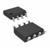
LMV932MA/NOPB National Semiconductor, LMV932MA/NOPB Datasheet - Page 7

LMV932MA/NOPB
Manufacturer Part Number
LMV932MA/NOPB
Description
IC OPAMP 1.8V DUAL RRIO 8SOIC
Manufacturer
National Semiconductor
Datasheet
1.LMV931MGNOPB.pdf
(20 pages)
Specifications of LMV932MA/NOPB
Amplifier Type
General Purpose
Number Of Circuits
2
Output Type
Rail-to-Rail
Slew Rate
0.42 V/µs
Gain Bandwidth Product
1.5MHz
Current - Input Bias
14nA
Voltage - Input Offset
1000µV
Current - Supply
116µA
Current - Output / Channel
100mA
Voltage - Supply, Single/dual (±)
1.8 V ~ 5.5 V, ±0.9 V ~ 2.75 V
Operating Temperature
-40°C ~ 125°C
Mounting Type
Surface Mount
Package / Case
8-SOIC (3.9mm Width)
Lead Free Status / RoHS Status
Lead free / RoHS Compliant
-3db Bandwidth
-
Other names
*LMV932MA
LMV932MA
LMV932MA
Available stocks
Company
Part Number
Manufacturer
Quantity
Price
Part Number:
LMV932MA/NOPB
Manufacturer:
NS/国半
Quantity:
20 000
SR
GBW
Φ
G
e
i
THD
n
Symbol
n
m
m
5V AC Electrical Characteristics
Unless otherwise specified, all limits guaranteed for T
Boldface limits apply at the temperature extremes. See
Note 1: Absolute Maximum Ratings indicate limits beyond which damage to the device may occur. Operating Ratings indicate conditions for which the device is
intended to be functional, but specific performance is not guaranteed. For guaranteed specifications and the test conditions, see the Electrical Characteristics.
Note 2: Human Body Model, applicable std. MIL-STD-883, Method 3015.7. Machine Model, applicable std. JESD22-A115-A (ESD MM std. of JEDEC)
Field-Induced Charge-Device Model, applicable std. JESD22-C101-C (ESD FICDM std. of JEDEC).
Note 3: Applies to both single-supply and split-supply operation. Continuous short circuit operation at elevated ambient temperature can result in exceeding the
maximum allowed junction temperature of 150°C. Output currents in excess of 45mA over long term may adversely affect reliability.
Note 4: The maximum power dissipation is a function of T
P
Note 5: Typical values represent the most likely parametric norm as determined at the time of characterization. Actual typical values may vary over time and will
also depend on the application and configuration. The typical values are not tested and are not guaranteed on shipped production material.
Note 6: All limits are guaranteed by testing or statistical analysis.
Note 7: Connected as voltage follower with input step from V
Note 8: For guaranteed temperature ranges, see Input Common-Mode Voltage Range specifications.
Note 9: Input referred, R
Note 10: Electrical Table values apply only for factory testing conditions at the temperature indicated. Factory testing conditions result in very limited self-heating
of the device such that T
T
the device may be permanently degraded, either mechanically or electrically.
D
A
. See Applications section for information of temperature derating of the device. Absolute Maximum Ratings indicated junction temperature limits beyond which
= (T
J(MAX)
Slew Rate
Gain-Bandwidth Product
Phase Margin
Gain Margin
Input-Referred Voltage Noise
Input-Referred Current Noise
Total Harmonic Distortion
Amp-to-Amp Isolation
– T
A
)/ θ
JA
. All numbers apply for packages soldered directly onto a PC Board.
J
Parameter
L
= T
= 100kΩ connected to V
A
. No guarantee of parametric performance is indicated in the electrical tables under conditions of internal self-heating where T
+
/2. Each amp excited in turn with 1kHz to produce V
(Note
f = 10 kHz, V
f = 10 kHz
f = 1kHz, A
R
(Note
L
= 600Ω, V
J(MAX)
7)
9)
−
to V
, θ
JA
J
V
+
Conditions
. Number specified is the slower of the positive and negative slew rates.
= 25°C. V
and T
= +1
CM
O
(Note
= 1V
= 1V
A
. The maximum allowable power dissipation at any ambient temperature is
10)
PP
7
+
= 5V, V
−
= 0V, V
(Note
Min
CM
O
= 3V
= V
6)
PP
+
/2, V
(For Supply Voltages <3V, V
(Note
O
0.022
0.42
0.08
Typ
123
1.5
71
50
= 2.5V and R
8
5)
(Note
Max
L
> 1 MΩ.
6)
O
= V
www.national.com
+
).
Units
V/µs
MHz
deg
dB
dB
%
J
>


