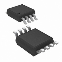
LMP7718MM/NOPB National Semiconductor, LMP7718MM/NOPB Datasheet - Page 15

LMP7718MM/NOPB
Manufacturer Part Number
LMP7718MM/NOPB
Description
IC OP AMP PREC DUAL 88MHZ 8MSOP
Manufacturer
National Semiconductor
Series
LMP®, PowerWise®r
Datasheet
1.LMP7717MFNOPB.pdf
(24 pages)
Specifications of LMP7718MM/NOPB
Amplifier Type
General Purpose
Number Of Circuits
2
Output Type
Rail-to-Rail
Slew Rate
35 V/µs
Gain Bandwidth Product
88MHz
Current - Input Bias
0.1pA
Voltage - Input Offset
10µV
Current - Supply
1.3mA
Current - Output / Channel
60mA
Voltage - Supply, Single/dual (±)
1.8 V ~ 5.5 V, ±0.9 V ~ 2.75 V
Operating Temperature
-40°C ~ 125°C
Mounting Type
Surface Mount
Package / Case
8-MSOP, Micro8™, 8-uMAX, 8-uSOP,
Lead Free Status / RoHS Status
Lead free / RoHS Compliant
-3db Bandwidth
-
Other names
LMP7718MM
LMP7718MM
LMP7718MMTR
LMP7718MM
LMP7718MMTR
The circuit gain for
F, the feedback factor is not equal to the circuit gain. The
feedback factor is derived from feedback theory and is the
same for both inverting and non-inverting configurations. Yes,
the feedback factor at low frequencies is equal to the gain for
the non-inverting configuration.
From this formula, we can see that
•
•
•
•
Please note the constraint 1/F
only in the vicinity where the open loop gain A and 1/F inter-
sect; 1/F can be shaped elsewhere as needed. The 1/F pole
must occur before the intersection with the open loop gain A.
In order to have adequate phase margin, it is desirable to fol-
low these two rules:
Rule 1 1/F and the open loop gain A should intersect at the
Rule 2 1/F’s pole should be set at least one decade below
Calculating Lead-Lag Compensation for LMP7717
Figure 5
curves have been redrawn as smooth lines to more readily
show the concepts covered, and to clearly show the key pa-
rameters used in the calculations for lead-lag compensation.
1/F's zero is located at a lower frequency compared with
1/F's pole.
1/F's value at low frequency is 1 + R
This method creates one additional pole and one
additional zero.
This pole-zero pair will serve two purposes:
— To raise the 1/F value at higher frequencies prior to its
— To achieve the previous purpose above with no
intercept with A, the open loop gain curve, in order to
meet the G
some overcompensation will be necessary for good
stability.
additional loop phase delay.
frequency where there is a minimum of 45° of phase
margin. When over-compensation is required the in-
tersection point of A and 1/F is set at a frequency
where the phase margin is above 45°, therefore in-
creasing the stability of the circuit.
the intersection with the open loop gain A in order to
take advantage of the full 90° of phase lead brought
by 1/F’s pole which is F’s zero. This ensures that the
effect of the zero is fully neutralized when the 1/F and
A plots intersect each other.
is the same plot as
min
Figure 4
= 10 requirement. For the LMP7717
at low frequencies is −R
Figure
≥
G
1, but the A
min
needs to be satisfied
F
/R
IN
.
VOL
and phase
F
/R
IN
, but
(4)
(5)
15
To obtain stable operation with gains under 10 V/V the open
loop gain margin must be reduced at high frequencies to
where there is a 45° phase margin when the gain margin of
the circuit with the external compensation is 0 dB. The pole
and zero in F, the feedback factor, control the gain margin at
the higher frequencies. The distance between F and A
the gain margin; therefore, the unity gain point (0 dB) is where
F crosses the A
For the example being used R
fore F = 6 dB at low frequencies. At the higher frequencies
the minimum value for F is 18 dB for 45° phase margin. From
Equation 5 we have the following relationship:
Now set R
we have R
the ratio between the resistors. Once the value of the resistors
is set, then the position of the pole in F must be set. A 2 kΩ
resistor is used for R
value for R
kΩ/5.9.
Rewriting Equation 2 to solve for the minimum capacitor value
gives the following equation:
The feedback factor curve, F, intersects the A
about 12 MHz. Therefore the pole of F should not be any
larger than 1.2 MHz. Using this value and R
minimum value for C is 390 pF.
too much overshoot, but the part is stable. Increasing C to 2.2
nF did not improve the ringing, as shown in
FIGURE 5. LMP7717/LMP7718 Simplified Bode Plot
F
C
C
= R
= R/5.9. Note that the value of C does not affect
is set at 330Ω, the closest standard value for 2
VOL
IN
= R. With these values and solving for R
curve.
F
C = 1/(2
and R
IN
IN
π
in this design. Therefore the
Figure 6
= R
f
p
R
C
F
)
for a gain of −1. There-
shows that there is
Figure
C
VOL
www.national.com
= 330Ω the
7.
curve at
30010848
VOL
is
C


