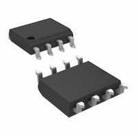
LMP7731MA/NOPB National Semiconductor, LMP7731MA/NOPB Datasheet - Page 6

LMP7731MA/NOPB
Manufacturer Part Number
LMP7731MA/NOPB
Description
IC AMP RRIO PREC SGL LN 8SOIC
Manufacturer
National Semiconductor
Series
LMP®, PowerWise®r
Datasheet
1.LMP7731MFNOPB.pdf
(18 pages)
Specifications of LMP7731MA/NOPB
Amplifier Type
General Purpose
Number Of Circuits
1
Output Type
Rail-to-Rail
Slew Rate
2.4 V/µs
Gain Bandwidth Product
22MHz
Current - Input Bias
14nA
Voltage - Input Offset
6µV
Current - Supply
2.5mA
Current - Output / Channel
49mA
Voltage - Supply, Single/dual (±)
1.8 V ~ 5.5 V
Operating Temperature
-40°C ~ 125°C
Mounting Type
Surface Mount
Package / Case
8-SOIC (3.9mm Width)
Number Of Channels
1
Voltage Gain Db
130 dB
Common Mode Rejection Ratio (min)
101 dB
Input Offset Voltage
0.5 mV at 5 V
Operating Supply Voltage
3 V, 5 V
Supply Current
3.4 mA at 5 V
Maximum Operating Temperature
+ 125 C
Minimum Operating Temperature
- 40 C
Lead Free Status / RoHS Status
Lead free / RoHS Compliant
-3db Bandwidth
-
Lead Free Status / Rohs Status
Details
Other names
*LMP7731MA/NOPB
LMP7731MA
LMP7731MA
www.national.com
G
Φ
R
THD+N
e
i
Symbol
n
n
IN
M
M
Note 1: Absolute Maximum Ratings indicate limits beyond which damage to the device may occur. Operating Ratings indicate conditions for which the device is
intended to be functional, but specific performance is not guaranteed. For guaranteed specifications and the test conditions, see the Electrical Characteristics
Tables.
Note 2: Human Body Model, applicable std. MIL-STD-883, Method 3015.7. Machine Model, applicable std. JESD22-A115-A (ESD MM std. of JEDEC)
Field-Induced Charge-Device Model, applicable std. JESD22-C101-C (ESD FICDM std. of JEDEC).
Note 3: The maximum power dissipation is a function of T
P
Note 4: Electrical Table values apply only for factory testing conditions at the temperature indicated. Factory testing conditions result in very limited self-heating
of the device such that T
T
Note 5: Typical values represent the most likely parametric norm as determined at the time of characterization. Actual typical values may vary over time and will
also depend on the application and configuration. The typical values are not tested and are not guaranteed on shipped production material.
Note 6: All limits are guaranteed by testing, statistical analysis or design.
Note 7: Ambient production test is performed at 25°C with a variance of ±3°C.
Connection Diagrams
Ordering Information
A
D
5-Pin SOT-23
. Absolute maximum Ratings indicate junction temperature limits beyond which the device maybe permanently degraded, either mechanically or electrically.
8-Pin SOIC
= (T
Package
J(MAX)
Gain Margin
Phase Margin
Input Resistance
Total Harmonic Distortion + Noise
Input Referred Voltage Noise Density
Input Voltage Noise
Input Referred Current Noise Density
– T
A
)/ θ
JA
. All numbers apply for packages soldered directly onto a PC Board.
J
= T
Parameter
LMP7731MAX
A
LMP7731MFE
LMP7731MFX
Part Number
LMP7731MF
LMP7731MA
. No guarantee of parametric performance is indicated in the electrical tables under conditions of internal self-heating where T
5-Pin SOT-23
Top View
20175202
J(MAX)
Package Marking
C
C
Differential Mode
Common Mode
A
f = 1 kHz, V
f = 1 kHz, V
0.1 Hz to 10 Hz
f = 1 kHz, V
f = 1 kHz, V
V
L
L
LMP7731MA
, θ
= 20 pF, R
= 20 pF, R
= 1, f = 1 kHz, Amplitude = 1V
JA
AY3A
. The maximum allowable power dissipation at any ambient temperature is
CM
CM
CM
CM
L
L
Conditions
= 4.5V
= 0.5V
= 4.5V
= 0.5V
6
= 10 kΩ to V
= 10 kΩ to V
+
+
/2
/2
1k Units Tape and Reel
250 Units Tape an Reel
3k Units Tape and Reel
2.5k Tape and Reel
Transport Media
95 Units/Rail
8-Pin SOIC
(Note 6)
Top View
Min
(Note 5)
0.001
Typ
151
2.9
2.9
1.1
2.2
12
65
38
78
(Note 6)
20175203
NSC Drawing
Max
MF05A
M08A
nV/
pA/
Units
nV
deg
MΩ
dB
kΩ
%
J
PP
>


