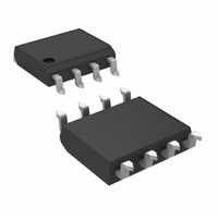
LMH6646MA/NOPB National Semiconductor, LMH6646MA/NOPB Datasheet - Page 14

LMH6646MA/NOPB
Manufacturer Part Number
LMH6646MA/NOPB
Description
IC AMP R-R I/O 2.7V 55MHZ 8-SOIC
Manufacturer
National Semiconductor
Series
PowerWise®, VIP10™r
Datasheet
1.LMH6647MF.pdf
(19 pages)
Specifications of LMH6646MA/NOPB
Amplifier Type
Voltage Feedback
Number Of Circuits
2
Output Type
Push-Pull, Rail-to-Rail
Slew Rate
22 V/µs
-3db Bandwidth
55MHz
Current - Input Bias
650nA
Voltage - Input Offset
1000µV
Current - Supply
725µA
Current - Output / Channel
20mA
Voltage - Supply, Single/dual (±)
2.5 V ~ 12 V, ±1.25 V ~ 6 V
Operating Temperature
-40°C ~ 85°C
Mounting Type
Surface Mount
Package / Case
8-SOIC (3.9mm Width)
Lead Free Status / RoHS Status
Lead free / RoHS Compliant
Gain Bandwidth Product
-
Other names
*LMH6646MA
*LMH6646MA/NOPB
LMH6646MA
*LMH6646MA/NOPB
LMH6646MA
Available stocks
Company
Part Number
Manufacturer
Quantity
Price
Part Number:
LMH6646MA/NOPB
Manufacturer:
NS/国半
Quantity:
20 000
www.national.com
Application Notes
CIRCUIT DESCRIPTION
The LMH6645/6646/6647 family is based on National Semi-
conductor’s proprietary VIP10 dielectrically isolated bipolar
process.
This device family architecture features the following:
APPLICATION HINTS
The total input common mode voltage range, which extends
from below V
a NPN stage. The NPN stage is switched on whenever the
input is less than 1.2V from V
rest of the range. In terms of the input voltage, there is an
overlapping region where both stages are processing the
input signal. This region is about 0.5V from beginning to the
end. As far as the device application is concerned, this
transition is a transparent operation. However, keep in mind
that the input bias current value and direction will depend on
which input stage is operating (see typical performance
characteristics for plots). For low distortion applications, it is
best to keep the input common mode voltage from transvers-
ing this transition point. Low gain settling applications, which
generally encounter larger peak-to-peak input voltages,
could be configured as inverting stages to eliminate common
mode voltage fluctuations.
In terms of the output, when the output swing approaches
either supply rail, the output transistor will enter a Quasi-
saturated state. A subtle effect of this operational region is
that there is an increase in supply current in this state (up to
1mA). The onset of Quasi-saturation region is a function of
output loading (current) and varies from 100mV at no load to
about 1V when output is delivering 20mA, as measured from
supplies. Both input common mode voltage and output volt-
age level effect the supply current (see typical performance
characteristics for plot).
With 2.7V supplies and a common mode input voltage range
that extends beyond either supply rail, the LMH6645/6646/
6647 family is well suited to many low voltage/low power
applications. Even with 2.7V supplies, the −3dB BW (
+1) is typically 55MHz with a tested limit of 45MHz. Produc-
tion testing guarantees that process variations will not com-
promise speed.
• Complimentary bipolar devices with exceptionally high f
• Rail-to-Rail input which allows the input common mode
• A class A-B “turn-around” stage with improved noise,
• Common Emitter push-pull output stage capable of 20mA
• Consistent performance from any supply voltage (2.7V-
(∼8GHz) even under low supply voltage (2.7V) and low
Collector bias current.
voltage to go beyond either rail by about 0.5V typically.
offset, and reduced power dissipation compared to simi-
lar speed devices (patent pending).
output current (at 0.5V from the supply rails) while con-
suming only ∼700µA of total supply current per channel.
This architecture allows output to reach within milli-volts
of either supply rail at light loads.
10V) with little variation with supply voltage for the most
important specifications (e.g. BW, SR, I
−
to beyond V
+
, is covered by both a PNP and
+
and the PNP stage covers the
OUT
, etc.)
@
A
V
=
t
14
This device family is designed to avoid output phase rever-
sal. With input over-drive, the output is kept near the supply
rail (or as close to it as mandated by the closed loop gain
setting and the input voltage). Figure 1, below, shows the
input and output voltage when the input voltage significantly
exceeds the supply voltages:
As can be seen, the output does not exhibit any phase
reversal as some op amps do. However, if the input voltage
range is exceeded by more than a diode drop beyond either
rail, the internal ESD protection diodes will start to conduct.
The current flow in these ESD diodes should be externally
limited.
LMH6647
MICRO-POWER SHUTDOWN
The LMH6647 can be shutdown to save power and reduce
its supply current to less than 50µA guaranteed, by applying
a voltage to the SD pin. The SD pin is “active high” and
needs to be tied to V
current (
to V
guaranteed when SD pin is 0.4V or less from V
operating supply voltage and temperature.
In the shutdown mode, essentially all internal device biasing
is turned off in order to minimize supply current flow and the
output goes into Hi-Z (high impedance) mode. Complete
device Turn-on and Turn-off times vary considerably relative
to the output loading conditions, output voltage, and input
impedance, but is generally limited to less than 1µs (see
tables for actual data).
FIGURE 1. Input/Output Shown with Exceeded Input
−
(≤20kΩ) will result in normal operation. Shutdown is
<
20µA, 4pF equivalent capacitance) and a resistor
−
for normal operation. This input is low
CMVR
20020233
+
at any


