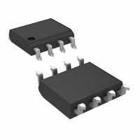
LM7171AIM/NOPB National Semiconductor, LM7171AIM/NOPB Datasheet

LM7171AIM/NOPB
Specifications of LM7171AIM/NOPB
*LM7171AIM/NOPB
LM7171AIM
Related parts for LM7171AIM/NOPB
LM7171AIM/NOPB Summary of contents
Page 1
... The LM7171 is built on National’s advanced VIP cally integrated PNP) complementary bipolar process. Typical Performance VIP ™ trademark of National Semiconductor Corporation. © 2006 National Semiconductor Corporation Features (Typical Unless Otherwise Noted) n Easy-to-use voltage feedback topology n Very high slew rate: n Wide unity-gain bandwidth: 200 MHz n − ...
Page 2
... Absolute Maximum Ratings If Military/Aerospace specified devices are required, please contact the National Semiconductor Sales Office/ Distributors for availability and specifications. ESD Tolerance (Note 2) + − Supply Voltage (V –V ) Differential Input Voltage (Note 11) Output Short Circuit to Ground (Note 3) Storage Temperature Range ± 15V DC Electrical Characteristics ...
Page 3
DC Electrical Characteristics Unless otherwise specified, all limits guaranteed for T limits apply at the temperature extremes Symbol Parameter Output Current (in Linear Region) I Output Short Circuit SC Current I Supply Current S ± 15V AC Electrical ...
Page 4
DC Electrical Characteristics Unless otherwise specified, all limits guaranteed for T apply at the temperature extremes Symbol Parameter R Input Resistance IN R Output Resistance O CMRR Common Mode Rejection Ratio PSRR Power Supply Rejection Ratio V Input ...
Page 5
AC Electrical Characteristics Unless otherwise specified 25˚ Symbol Parameter Second Harmonic (Note 12) Third Harmonic (Note 12) e Input-Referred n Voltage Noise i Input-Referred n Current Noise Note 1: Absolute Maximum Ratings indicate limits ...
Page 6
Typical Performance Characteristics Supply Current vs. Supply Voltage Input Offset Voltage vs. Temperature Short Circuit Current vs. Temperature (Sourcing) www.national.com unless otherwise noted, T Supply Current vs. Temperature 01238563 Input Bias Current vs. Temperature 01238565 Short Circuit Current vs. Temperature ...
Page 7
Typical Performance Characteristics Output Voltage vs. Output Current CMRR vs. Frequency PSRR vs. Frequency unless otherwise noted, T Output Voltage vs. Output Current 01238569 PSRR vs. Frequency 01238571 Open Loop Frequency Response 01238573 7 = 25˚C (Continued) A 01238570 01238572 ...
Page 8
Typical Performance Characteristics Open Loop Frequency Response Gain-Bandwidth Product vs. Load Capacitance Large Signal Voltage Gain vs. Load www.national.com unless otherwise noted, T Gain-Bandwidth Product vs. Supply Voltage 01238552 Large Signal Voltage Gain vs. Load 01238554 Input Voltage Noise vs. ...
Page 9
Typical Performance Characteristics Input Voltage Noise vs. Frequency Input Current Noise vs. Frequency Slew Rate vs. Input Voltage unless otherwise noted, T Input Current Noise vs. Frequency 01238558 Slew Rate vs. Supply Voltage 01238560 Slew Rate vs. Load Capacitance 01238562 ...
Page 10
Typical Performance Characteristics Open Loop Output Impedance vs. Frequency Large Signal Pulse Response ± − Large Signal Pulse Response ± + www.national.com unless otherwise noted, T Open Loop ...
Page 11
Typical Performance Characteristics Small Signal Pulse Response ± − 15V V S Small Signal Pulse Response ± + 15V V S Closed Loop Frequency Response vs. Supply Voltage (A = +2) V ...
Page 12
Typical Performance Characteristics Closed Loop Frequency Response vs. Capacitive Load (A = +2) V Closed Loop Frequency Response vs. Input Signal Level (A = +2) V Closed Loop Frequency Response vs. Input Signal Level (A = +2) V www.national.com unless ...
Page 13
Typical Performance Characteristics Closed Loop Frequency Response vs. Input Signal Level (A = +4) V Closed Loop Frequency Response vs. Input Signal Level (A = +4) V Total Harmonic Distortion vs. Frequency (Note 13) unless otherwise noted, T Closed Loop ...
Page 14
Typical Performance Characteristics Undistorted Output Swing vs. Frequency Harmonic Distortion vs. Frequency (Note 13) Maximum Power Dissipation vs. Ambient Temperature www.national.com unless otherwise noted Undistorted Output Swing vs. Frequency 01238548 Harmonic Distortion vs. Frequency (Note 13) 01238574 01238520 ...
Page 15
Simplified Schematic Diagram Note: M1 and M2 are current mirrors. 15 01238509 www.national.com ...
Page 16
Application Notes PERFORMANCE DISCUSSION The LM7171 is a very high speed, voltage feedback ampli- fier. It consumes only 6.5 mA supply current while providing a unity-gain bandwidth of 200 MHz and a slew rate of 4100V/µs. It also has other ...
Page 17
Application Notes (Continued) ally by placing 0.01 µF ceramic capacitors directly to power supply pins and 2.2 µF tantalum capacitors close to the power supply pins. 01238511 FIGURE 2. Power Supply Bypassing TERMINATION In high frequency applications, reflections occur if ...
Page 18
Application Notes (Continued) Thermal resistance, θ , depends on parameters such as JA die size, package size and package material. The smaller the die size and package, the higher θ DIP package has a lower thermal resistance (108˚C/W) than that ...
Page 19
Physical Dimensions inches (millimeters) unless otherwise noted 8-Pin SOIC NS Package Number M08A 8-Pin MDIP NS Package Number N08E 19 www.national.com ...
Page 20
... BANNED SUBSTANCE COMPLIANCE National Semiconductor follows the provisions of the Product Stewardship Guide for Customers (CSP-9-111C2) and Banned Substances and Materials of Interest Specification (CSP-9-111S2) for regulatory environmental compliance. Details may be found at: www.national.com/quality/green. ...


