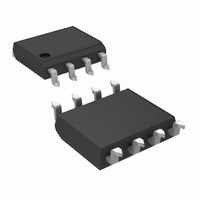
LM6142AIM/NOPB National Semiconductor, LM6142AIM/NOPB Datasheet - Page 11

LM6142AIM/NOPB
Manufacturer Part Number
LM6142AIM/NOPB
Description
IC OP AMP DUAL HS R-R 8-SOIC
Manufacturer
National Semiconductor
Specifications of LM6142AIM/NOPB
Amplifier Type
General Purpose
Number Of Circuits
2
Output Type
Rail-to-Rail
Slew Rate
25 V/µs
Gain Bandwidth Product
9MHz
Current - Input Bias
174nA
Voltage - Input Offset
1300µV
Current - Supply
750µA
Current - Output / Channel
24mA
Voltage - Supply, Single/dual (±)
1.8 V ~ 24 V, ±0.9 V ~ 12 V
Operating Temperature
-40°C ~ 85°C
Mounting Type
Surface Mount
Package / Case
8-SOIC (3.9mm Width)
Bandwidth
17 MHz
Channel Separation
130
Common Mode Rejection Ratio
82
Current, Input Bias
180 nA
Current, Input Offset
3 nA
Current, Output
13 mA
Current, Supply
650 μA
Harmonic Distortion
0.003 %
Impedance, Thermal
193 °C/W
Number Of Amplifiers
Dual
Package Type
SO-8
Resistance, Input
126 Megohms
Temperature, Operating, Range
-40 to +85 °C
Voltage, Gain
270 V/mV
Voltage, Input
1.8 to 24 V
Voltage, Noise
16 nV/sqrt Hz
Voltage, Offset
0.3 mV
Voltage, Output, High
4.995 V
Voltage, Output, Low
0.005 V
Voltage, Supply
5 V
Lead Free Status / RoHS Status
Lead free / RoHS Compliant
-3db Bandwidth
-
Lead Free Status / Rohs Status
RoHS Compliant part
Electrostatic Device
Other names
*LM6142AIM
*LM6142AIM/NOPB
LM6142AIM
*LM6142AIM/NOPB
LM6142AIM
Typical Performance Characteristics
Specified (Continued)
LM6142/LM6144 Application Ideas
The LM6142 brings a new level of ease of use to op amp
system design.
With greater than rail-to-rail input voltage range concern
over exceeding the common-mode voltage range is elimi-
nated.
Rail-to-rail output swing provides the maximum possible dy-
namic range at the output. This is particularly important
when operating on low supply voltages.
The high gain-bandwidth with low supply current opens new
battery powered applications, where high power consump-
tion, previously reduced battery life to unacceptable levels.
To take advantage of these features, some ideas should be
kept in mind.
ENHANCED SLEW RATE
Unlike most bipolar op amps, the unique phase reversal
prevention/speed-up circuit in the input stage causes the
slew rate to be very much a function of the input signal
amplitude.
Figure 2 shows how excess input signal, is routed around
the input collector-base junctions, directly to the current
mirrors.
The LM6142/LM6144 input stage converts the input voltage
change to a current change. This current change drives the
current mirrors through the collectors of Q1–Q2, Q3–Q4
when the input levels are normal.
If the input signal exceeds the slew rate of the input stage,
the differential input voltage rises above two diode drops.
This excess signal bypasses the normal input transistors,
(Q1–Q4), and is routed in correct phase through the two
additional transistors, (Q5, Q6), directly into the current mir-
rors.
This rerouting of excess signal allows the slew-rate to in-
crease by a factor of 10 to 1 or more. (See Figure 1.)
As the overdrive increases, the op amp reacts better than a
conventional op amp. Large fast pulses will raise the slew-
rate to around 30V to 60V/µs.
Noise Current vs. Frequency
01205745
T
11
A
= 25˚C, R
This effect is most noticeable at higher supply voltages and
lower gains where incoming signals are likely to be large.
This new input circuit also eliminates the phase reversal
seen in many op amps when they are overdriven.
This speed-up action adds stability to the system when
driving large capacitive loads.
DRIVING CAPACITIVE LOADS
Capacitive loads decrease the phase margin of all op amps.
This is caused by the output resistance of the amplifier and
the load capacitance forming an R-C phase lag network.
This can lead to overshoot, ringing and oscillation. Slew rate
limiting can also cause additional lag. Most op amps with a
fixed maximum slew-rate will lag further and further behind
when driving capacitive loads even though the differential
input voltage raises. With the LM6142, the lag causes the
slew rate to raise. The increased slew-rate keeps the output
following the input much better. This effectively reduces
phase lag. After the output has caught up with the input, the
differential input voltage drops down and the amplifier settles
rapidly.
L
= 10 kΩ Unless Otherwise
Slew Rate vs. ∆ V
NF vs. R
FIGURE 1.
V
S
=
Source
±
5V
IN
01205712
01205707
www.national.com


