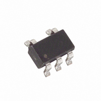
MAX4250EUK+T Maxim Integrated Products, MAX4250EUK+T Datasheet - Page 11

MAX4250EUK+T
Manufacturer Part Number
MAX4250EUK+T
Description
IC OP AMP R-R LN SOT23-5
Manufacturer
Maxim Integrated Products
Datasheet
1.MAX4252EBLT.pdf
(19 pages)
Specifications of MAX4250EUK+T
Amplifier Type
General Purpose
Number Of Circuits
1
Output Type
Push-Pull, Rail-to-Rail
Slew Rate
0.3 V/µs
Gain Bandwidth Product
3MHz
Current - Input Bias
1pA
Voltage - Input Offset
70µV
Current - Supply
420µA
Current - Output / Channel
68mA
Voltage - Supply, Single/dual (±)
2.4 V ~ 5.5 V, ±1.2 V ~ 2.75 V
Operating Temperature
-40°C ~ 85°C
Mounting Type
Surface Mount
Package / Case
SOT-23-5, SC-74A, SOT-25
Number Of Channels
1
Voltage Gain Db
116 dB
Common Mode Rejection Ratio (min)
70 dB
Input Offset Voltage
0.07 mV
Operating Supply Voltage
3 V, 5 V
Maximum Power Dissipation
571 mW
Maximum Operating Temperature
+ 85 C
Mounting Style
SMD/SMT
Maximum Dual Supply Voltage
+/- 2.75 V
Minimum Operating Temperature
- 40 C
Lead Free Status / RoHS Status
Lead free / RoHS Compliant
-3db Bandwidth
-
Lead Free Status / Rohs Status
Details
Other names
MAX4250EUK+T
MAX4250EUK+TTR
MAX4250EUK+TTR
Figure 3. Overdriven Input Showing No Phase Reversal
Figure 4. Rail-to-Rail Output Operation
Figure 5. Capacitive-Load Driving Circuit
4.45V
V
4.25V
IN
0
0
5V
0
V
R
A
f = 1kHz
DD
L
V
= 10
= 10k
= 5V
______________________________________________________________________________________
200 s/div
20 s/div
MAX4250
MAX4251
MAX4252
MAX4253
MAX4254
Low-Distortion, Rail-to-Rail Op Amps
R
ISO
A
V
R
V
DD
L
= 1
= 10k
UCSP, Single-Supply, Low-Noise,
= 5V
-200mV
V
V
V
1V/div
OUT
IN
C
OUT
L
V
OUT
The amplifier’s input capacitance is 11pF. If the resis-
tance seen by the inverting input is large (feedback
network), this can introduce a pole within the amplifier’s
bandwidth, resulting in reduced phase margin.
Compensate the reduced phase margin by introducing
a feed-forward capacitor (C
input and the output (Figure 1). This effectively cancels
the pole from the inverting input of the amplifier.
Choose the value of C
In the unity-gain stable MAX4250–MAX4254, the use of
a proper C
A
MAX4255/MAX4256/MAX4257, C
for A
response both with and without C
Using a slightly smaller C
mula above achieves a higher bandwidth at the
expense of reduced phase and gain margin. As a gen-
eral guideline, consider using C
R
greater than 5k
MAX4257).
The MAX4249–MAX4257 combine good driving capa-
bility with ground-sensing input and rail-to-rail output
operation. With their low distortion, low noise, and low-
power consumption, these devices are ideal for use in
portable instrumentation systems and other low-power,
noise-sensitive applications.
The common-mode input range of these devices
extends below ground, and offers excellent common-
mode rejection. These devices are guaranteed not to
undergo phase reversal when the input is overdriven
(Figure 3).
Figure 4 showcases the true rail-to-rail output operation
of the amplifier, configured with A
swings to within 8mV of the supplies with a 10k
making the devices ideal in low-supply-voltage applica-
tions.
Even with their low quiescent current of 400µA, these
amplifiers can drive 1k
lent DC accuracy. Stability while driving heavy capaci-
tive loads is another key feature.
V
F
Ground-Sensing and Rail-to-Rail Outputs
is greater than 20k
= -1V/V. In the decompensated MAX4249/
V
= 10V/V. Figures 2a and 2b show transient
Using a Feed-Forward Compensation
Z
is most important for A
Applications Information
C
Z
Output Loading and Stability
= 11 x (R
(MAX4249/MAX4255/MAX4256/
Z
as follows:
loads while maintaining excel-
Z
than suggested by the for-
(MAX4250–MAX4254) or
F
Z
/ R
) between the inverting
Z
G
Z
V
for cases where R
) [pF]
Z
.
= 10V/V. The output
is most important
Capacitor, C
V
= 2V/V, and
load,
G
11
Z
||


