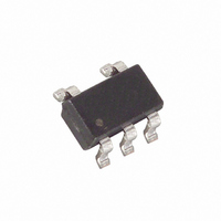
MAX4250EUK+T Maxim Integrated Products, MAX4250EUK+T Datasheet - Page 12

MAX4250EUK+T
Manufacturer Part Number
MAX4250EUK+T
Description
IC OP AMP R-R LN SOT23-5
Manufacturer
Maxim Integrated Products
Datasheet
1.MAX4252EBLT.pdf
(19 pages)
Specifications of MAX4250EUK+T
Amplifier Type
General Purpose
Number Of Circuits
1
Output Type
Push-Pull, Rail-to-Rail
Slew Rate
0.3 V/µs
Gain Bandwidth Product
3MHz
Current - Input Bias
1pA
Voltage - Input Offset
70µV
Current - Supply
420µA
Current - Output / Channel
68mA
Voltage - Supply, Single/dual (±)
2.4 V ~ 5.5 V, ±1.2 V ~ 2.75 V
Operating Temperature
-40°C ~ 85°C
Mounting Type
Surface Mount
Package / Case
SOT-23-5, SC-74A, SOT-25
Number Of Channels
1
Voltage Gain Db
116 dB
Common Mode Rejection Ratio (min)
70 dB
Input Offset Voltage
0.07 mV
Operating Supply Voltage
3 V, 5 V
Maximum Power Dissipation
571 mW
Maximum Operating Temperature
+ 85 C
Mounting Style
SMD/SMT
Maximum Dual Supply Voltage
+/- 2.75 V
Minimum Operating Temperature
- 40 C
Lead Free Status / RoHS Status
Lead free / RoHS Compliant
-3db Bandwidth
-
Lead Free Status / Rohs Status
Details
Other names
MAX4250EUK+T
MAX4250EUK+TTR
MAX4250EUK+TTR
These devices maintain stability while driving loads up
to 400pF. To drive higher capacitive loads, place a
small isolation resistor in series between the output of
the amplifier and the capacitive load (Figure 5). This
resistor improves the amplifier’s phase margin by isolat-
ing the capacitor from the op amp’s output. Reference
Figure 6 to select a resistance value that will ensure a
load capacitance that limits peaking to <2dB (25%).
UCSP, Single-Supply, Low-Noise,
Low-Distortion, Rail-to-Rail Op Amps
Figure 6. Isolation Resistance vs. Capacitive Loading to
Minimize Peaking (<2dB)
12
Figure 7. Peaking vs. Capacitive Load
______________________________________________________________________________________
160
140
120
100
25
20
15
10
NOTE: USING AN ISOLATION RESISTOR REDUCES PEAKING.
80
60
40
20
5
0
0
10
10
MAX4250–MAX4254 (A
MAX4249/MAX4255–MAX4257 (A
R
SHADED AREA INDICATES
STABLE OPERATION
WITH NO NEED FOR
ISOLATION RESISTOR.
ISO
= 0
CAPACITIVE LOADING (pF)
CAPACITIVE LOAD (pF)
100
100
SHADED AREA INDICATES
STABLE OPERATION
WITH NO NEED FOR
ISOLATION RESISTOR.
V
= 1)
1000
1000
V
= 10)
10,000
10,000
For example, if the capacitive load is 1000pF, the corre-
sponding isolation resistor is 150 . Figure 7 shows that
peaking occurs without the isolation resistor. Figure 8
shows the unity-gain bandwidth vs. capacitive load for
the MAX4250–MAX4254.
The MAX4249–MAX4257 operate from a single 2.4V to
5.5V power supply or from dual supplies of ±1.20V to
±2.75V. For single-supply operation, bypass the power
supply with a 0.1µF ceramic capacitor placed close to
the V
each supply to ground.
Good layout improves performance by decreasing the
amount of stray capacitance and noise at the op amp’s
inputs and output. To decrease stray capacitance, min-
imize PC board trace lengths and resistor leads, and
place external components close to the op amp’s pins.
For the latest application details on UCSP construction,
dimensions, tape carrier information, PC board tech-
niques, bump-pad layout, and recommended reflow
temperature profile, as well as the latest information on
reliability testing results, refer to the Application Note:
UCSP—A Wafer-Level Chip-Scale Package on Maxim’s
web site at www.maxim-ic.com/ucsp.
Figure 8. MAX4250–MAX4254 Unity-Gain Bandwidth vs.
Capacitive Load
DD
UCSP Applications Information
pin. If operating from dual supplies, bypass
4.5
4.0
3.5
3.0
2.5
2.0
1.5
1.0
0.5
0
10
SHADED AREA INDICATES
STABLE OPERATION
WITH NO NEED FOR
ISOLATION RESISTOR.
NOTE: R
Power Supplies and Layout
CAPACITIVE LOAD (pF)
ISO
100
CHOSEN FOR PEAKING 2dB.
1000
V
DD
= 3V
10,000


