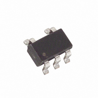
MAX4250EUK+T Maxim Integrated Products, MAX4250EUK+T Datasheet - Page 4

MAX4250EUK+T
Manufacturer Part Number
MAX4250EUK+T
Description
IC OP AMP R-R LN SOT23-5
Manufacturer
Maxim Integrated Products
Datasheet
1.MAX4252EBLT.pdf
(19 pages)
Specifications of MAX4250EUK+T
Amplifier Type
General Purpose
Number Of Circuits
1
Output Type
Push-Pull, Rail-to-Rail
Slew Rate
0.3 V/µs
Gain Bandwidth Product
3MHz
Current - Input Bias
1pA
Voltage - Input Offset
70µV
Current - Supply
420µA
Current - Output / Channel
68mA
Voltage - Supply, Single/dual (±)
2.4 V ~ 5.5 V, ±1.2 V ~ 2.75 V
Operating Temperature
-40°C ~ 85°C
Mounting Type
Surface Mount
Package / Case
SOT-23-5, SC-74A, SOT-25
Number Of Channels
1
Voltage Gain Db
116 dB
Common Mode Rejection Ratio (min)
70 dB
Input Offset Voltage
0.07 mV
Operating Supply Voltage
3 V, 5 V
Maximum Power Dissipation
571 mW
Maximum Operating Temperature
+ 85 C
Mounting Style
SMD/SMT
Maximum Dual Supply Voltage
+/- 2.75 V
Minimum Operating Temperature
- 40 C
Lead Free Status / RoHS Status
Lead free / RoHS Compliant
-3db Bandwidth
-
Lead Free Status / Rohs Status
Details
Other names
MAX4250EUK+T
MAX4250EUK+TTR
MAX4250EUK+TTR
ELECTRICAL CHARACTERISTICS (continued)
(V
ues are at T
UCSP, Single-Supply, Low-Noise,
Low-Distortion, Rail-to-Rail Op Amps
4
Note 2: SHDN is available on the MAX4249/MAX4251/MAX4253/MAX4256 only.
Note 3: All device specifications are 100% tested at T
Note 4: Guaranteed by the PSRR test.
Note 5: Offset voltage prior to reflow on the UCSP.
Note 6: Guaranteed by design.
Note 7: Lowpass-filter bandwidth is 22kHz for f = 1kHz and 80kHz for f = 20kHz. Noise floor of test equipment = 10nV/ Hz.
Total Harmonic Distortion Plus
Noise
Capacitive-Load Stability
Gain Margin
Phase Margin
Settling Time
Delay Time to Shutdown
Delay Time to Enable
Power-Up Delay Time
DD
_______________________________________________________________________________________
= 5V, V
PARAMETER
A
SS
= +25°C.) (Notes 2, 3)
= 0, V
CM
= 0, V
OUT
= V
SYMBOL
THD+N
GM
DD
t
t
t
SH
EN
PU
M
/2, R
L
MAX4250–MAX4254
A
R
(Note 7)
MAX4249/MAX4255/
MAX4256/MAX4257
A
R
No sustained oscillations
MAX4250–MAX4254, A
MAX4249/MAX4255/MAX4256/MAX4257,
A
MAX4250–MAX4254, A
MAX4249/MAX4255/MAX4256/MAX4257,
A
To 0.01%, V
= 2V step
I
normal
operation
V
V
0.1%
V
tied to V
VDD
OUT
OUT
DD
V
L
V
L
V
V
= 1kΩ to GND
= 1kΩ to GND (Note 7)
= 1V/V, V
= 1V/V, V
= 10V/V
= 10V/V
= 0 to 5V step, V
= 5% of
settles to
= 2.5V,
A
= +25°C. Limits over temperature are guaranteed by design.
DD
/2, SHDN = V
OUT
OUT
OUT
CONDITIONS
= 2V
= 2V
MAX4250–MAX4254
MAX4249/MAX4255/
MAX4256/MAX4257
MAX4251/MAX4253
MAX4249/MAX4256
MAX4251/MAX4253
MAX4249/MAX4256
OUT
P-P
P-P
V
V
,
,
= 1V/V
= 1V/V
DD
stable to 0.1%
, T
f = 1kHz
f = 20kHz
f = 1kHz
f = 20kHz
A
= T
MIN
to T
MAX
MIN
, unless otherwise noted. Typical val-
0.0004
0.0012
0.006
0.007
TYP
12.5
400
6.7
1.6
0.8
1.2
3.5
10
74
68
8
6
MAX
Degrees
UNITS
pF
dB
µs
µs
µs
µs
%


