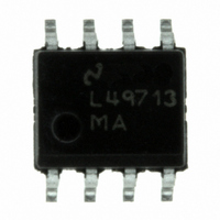
LME49713MA/NOPB National Semiconductor, LME49713MA/NOPB Datasheet - Page 10

LME49713MA/NOPB
Manufacturer Part Number
LME49713MA/NOPB
Description
IC AMP AUDIO MONO AB HIFI 8SOIC
Manufacturer
National Semiconductor
Datasheet
1.LME49713MABD.pdf
(14 pages)
Specifications of LME49713MA/NOPB
Amplifier Type
Audio
Number Of Circuits
1
Slew Rate
1900 V/µs
Gain Bandwidth Product
132MHz
Current - Input Bias
1.8µA
Voltage - Input Offset
50µV
Current - Supply
8mA
Current - Output / Channel
100mA
Voltage - Supply, Single/dual (±)
±5 V ~ 18 V
Operating Temperature
-40°C ~ 85°C
Mounting Type
Surface Mount
Package / Case
8-SOIC (3.9mm Width)
Amplifier Class
AB
No. Of Channels
1
Supply Voltage Range
± 5V To ± 18V
Load Impedance
2kohm
Operating Temperature Range
-40°C To +85°C
Amplifier Case Style
SOIC
No. Of Pins
8
Rohs Compliant
Yes
Number Of Channels
1
Common Mode Rejection Ratio (min)
86 dB
Input Offset Voltage
1 mV at +/- 15 V
Maximum Operating Temperature
+ 85 C
Maximum Dual Supply Voltage
+/- 18 V
Minimum Operating Temperature
- 40 C
For Use With
LME49713MABD - BOARD EVAL FOR LME49713MA
Lead Free Status / RoHS Status
Lead free / RoHS Compliant
Output Type
-
-3db Bandwidth
-
Lead Free Status / Rohs Status
Details
Other names
LME49713MA
www.national.com
Application Information
GENERAL AMPLIFIER FUNCTION
Voltage feedback amplifiers have a small-signal bandwidth
that is a function of the closed-loop gain. Conversely, the
LME49713 current feedback amplifier features a small-signal
bandwidth that is relatively independent of the closed-loop
gain. This is shown in Figure 1 where the LME49713’s gain
is –1,–2, –5 and –10. Like all current feedback amplifiers, the
LME49713’s closed-loop bandwidth is a function of the feed-
back resistance value. Therefore, R
the desired closed-loop gain.
POWER SUPPLY BYPASSING AND LAYOUT
CONSIDERATIONS
Properly placed and correctly valued supply bypassing is es-
sential for optimized high-speed amplifier operation. The sup-
ply bypassing must maintain a wideband, low-impedance
capacitive connection between the amplifier’s supply pin and
ground. This helps preserve high speed signal and fast tran-
sient fidelity. The bypassing is easily accomplished using a
parallel combination of a 10μF tantalum and a 0.1μF ceramic
capacitors for each power supply pin. The bypass capacitors
should be placed as close to the amplifier power supply pins
as possible.
FEEDBACK RESISTOR SELECTION (R
The value of the R
the LME49713. For general applications, the LME49713 will
maintain specified performance with an 1.2kΩ feedback re-
sistor. Although this value will provide good results for most
applications, it may be advantageous to adjust this value
slightly for best pulse response optimized for the desired
bandwidth. In addition to reducing bandwidth, increasing the
feedback resistor value also reduces overshoot in the time
domain response.
FIGURE 1. Bandwidth as a function of gain
f
, is also a dominant factor in compensating
s
must be varied to select
f
)
20213209
10
SLEW RATE CONSIDERATIONS
A current feedback amplifier’s slew rate characteristics are
different than that of voltage feedback amplifiers. A voltage
feedback amplifier’s slew rate limiting or non-linear amplifier
behavior is dominated by the finite availability of the first stage
tail current charging the second stage voltage amplifier’s
compensation capacitor. Conversely, a current feedback
amplifier’s slew rate is not constant. Transient current at the
inverting input determines slew rate for both inverting and
non-inverting gains. The non-inverting configuration slew rate
is also determined by input stage limitations. Accordingly,
variations of slew rates occur for different circuit topologies.
DRIVING CAPACITIVE LOADS
The LME49713 can drive significantly higher capacitive loads
than many current feedback amplifiers. Although the
LME49713 can directly drive as much as 100pF without os-
cillating, the resulting response will be a function of the feed-
back resistor value.
CAPACITIVE FEEDBACK
It is quite common to place a small lead-compensation ca-
pacitor in parallel with a voltage feedback amplifier’s feedback
resistance, R
peaking in the frequency domain and damps the transient re-
sponse. Whereas this yields the expected results when used
with voltage feedback amplifiers, this technique must not be
used with current feedback amplifiers. The dynamic
impedance of capacitors in the feedback loop reduces the
amplifier’s stability. Instead, reduced peaking in the frequency
response and bandwidth limiting can be accomplished by
adding an RC circuit to the amplifier’s input.
f
. This compensation reduces the amplifier’s


