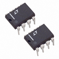
LT1055CN8 Linear Technology, LT1055CN8 Datasheet - Page 5

LT1055CN8
Manufacturer Part Number
LT1055CN8
Description
IC PREC OP-AMP JFET HI-SPD 8-DIP
Manufacturer
Linear Technology
Datasheet
1.LT1055CN8PBF.pdf
(16 pages)
Specifications of LT1055CN8
Amplifier Type
J-FET
Number Of Circuits
1
Slew Rate
12 V/µs
Gain Bandwidth Product
4.5MHz
Current - Input Bias
30pA
Voltage - Input Offset
120µV
Current - Supply
2.8mA
Voltage - Supply, Single/dual (±)
±5 V ~ 18 V
Operating Temperature
0°C ~ 70°C
Mounting Type
Through Hole
Package / Case
8-DIP (0.300", 7.62mm)
Lead Free Status / RoHS Status
Contains lead / RoHS non-compliant
Output Type
-
Current - Output / Channel
-
-3db Bandwidth
-
Available stocks
Company
Part Number
Manufacturer
Quantity
Price
Company:
Part Number:
LT1055CN8
Manufacturer:
LT
Quantity:
1 831
Company:
Part Number:
LT1055CN8
Manufacturer:
SIEMENS
Quantity:
1 835
Company:
Part Number:
LT1055CN8#PBF
Manufacturer:
LT
Quantity:
584
0°C ≤ T
SYMBOL PARAMETER
V
I
I
A
CMRR
PSRR
V
For MIL-STD components, please refer to LTC883 data sheet for test
listing and parameters.
Note 1: Stresses beyond those listed under Absolute Maximum Ratings
may cause permanent damage to the device. Exposure to any Absolute
Maximum Rating condition for extended periods may affect device
reliability and lifetime.
Note 2: Offset voltage is measured under two different conditions:
(a) approximately 0.5 seconds after application of power; (b) at T
only, with the chip heated to approximately 38°C for the LT1055 and to
45°C for the LT1056, to account for chip temperature rise when the device
is fully warmed up.
ELECTRICAL CHARACTERISTICS
OS
B
OS
VOL
OUT
A
≤ 70°C. V
Input Offset Voltage (Note 2)
Average Temperature Coefficient of Input Offset Voltage
Input Offset Current
Input Bias Current
Large-Signal Voltage Gain
Common Mode Rejection Ratio
Power Supply Rejection Ratio
Output Voltage Swing
S
= ±15V, V
CM
= 0V, unless otherwise noted.
A
= 25°C
The
CONDITIONS
Warmed Up, T
Warmed Up, T
V
V
V
R
●
O
CM
S
L
= ±10V, R
= ±10V to ±18V
= 2K
denotes the specifications which apply over the temperature range
= ±10.5V
Note 3: 10Hz noise voltage density is sample tested on every lot of A
grades. Devices 100% tested at 10Hz are available on request.
Note 4: This parameter is tested on a sample basis only.
Note 5: Current noise is calculated from the formula: i
q = 1.6 • 10
the contribution of current noise.
Note 6: Offset voltage drift with temperature is practically unchanged
when the offset voltage is trimmed to zero with a 100k potentiometer
between the balance terminals and the wiper tied to V
tighter drift specifications are available on request.
L
A
A
= 2k
= 70°C
= 70°C
–19
coulomb. The noise of source resistors up to 1GΩ swamps
●
●
●
●
●
●
●
●
MIN
±12
60
82
87
LT1055CS8/LT1056CS8
LT1055/LT1056
±13.1
TYP
±60
800
250
103
18
98
4
+
n
. Devices tested to
= (2ql
2200
±400
MAX
150
15
B
)
1/2
, where
UNITS
10556fc
µV/°C
V/mV
5
µV
pA
pA
dB
dB
V


