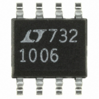
LT1006S8 Linear Technology, LT1006S8 Datasheet - Page 10

LT1006S8
Manufacturer Part Number
LT1006S8
Description
IC PREC OP-AMP 5V SINGLE 8-SOIC
Manufacturer
Linear Technology
Datasheet
1.LT1006CN8PBF.pdf
(16 pages)
Specifications of LT1006S8
Amplifier Type
General Purpose
Number Of Circuits
1
Slew Rate
1.2 V/µs
Current - Input Bias
10nA
Voltage - Input Offset
80µV
Current - Supply
360µA
Voltage - Supply, Single/dual (±)
5 V ~ 30 V, ±2.5 V ~ 15 V
Operating Temperature
0°C ~ 70°C
Mounting Type
Surface Mount
Package / Case
8-SOIC (3.9mm Width)
Lead Free Status / RoHS Status
Contains lead / RoHS non-compliant
Output Type
-
Current - Output / Channel
-
-3db Bandwidth
-
Gain Bandwidth Product
-
Available stocks
Company
Part Number
Manufacturer
Quantity
Price
Company:
Part Number:
LT1006S8
Manufacturer:
LT
Quantity:
10 000
Part Number:
LT1006S8
Manufacturer:
LINEAR/凌特
Quantity:
20 000
Company:
Part Number:
LT1006S8#PBF
Manufacturer:
LT
Quantity:
8 872
Part Number:
LT1006S8#PBF
Manufacturer:
LINEAR/凌特
Quantity:
20 000
Company:
Part Number:
LT1006S8#TR
Manufacturer:
LT
Quantity:
12
Company:
Part Number:
LT1006S8#TRPBF
Manufacturer:
LT
Quantity:
4 300
Part Number:
LT1006S8#TRPBF
Manufacturer:
LINEAR/凌特
Quantity:
20 000
Company:
Part Number:
LT1006S8TR
Manufacturer:
PHIL
Quantity:
4 580
APPLICATIO S I FOR ATIO
LT1006
In automated production testing the output is forced to
1.4V by the test loop; offset voltage is measured with a
common mode voltage of zero and the negative supply at
zero (Pin 4). Without the test loop, these exact conditions
cannot be achieved. The test circuit shown ensures that
the output will never saturate even with worst-case offset
voltages (– 250µV over the – 55°C to 125°C range). The
effective common mode input is 0.3V with respect to the
negative supply. As indicated by the common mode rejec-
tion specifications the difference is only a few microvolts
between the two methods of offset voltage measurement.
10
OUTPUT (V)
INPUT (mV)
–100
4
2
0
0
V
S
100Ω
50k*
= 5V, 0V
Test Circuit for Offset Voltage and
Offset Drift with Temperature
Comparator Rise Response Time
to 10mV, 5mV, 2mV Overdrives
U
–
+
**
*
LT1006
RESISTORS MUST HAVE LOW
THERMOELECTRIC POTENTIAL.
THIS CIRCUIT IS ALSO USED AS
THE BURN-IN CONFIGURATION,
WITH SUPPLY VOLTAGES
INCREASED TO ± 20V
V
O
50µs/DIV
U
– 0.3V
4.7V
50k*
= 1000V
OS
W
LT1006 • TA04
1006 TA12a
V
0
U
INPUT (mV) –100
OUTPUT (V)
Low Supply Operation
The minimum guaranteed supply voltage for proper
operation of the LT1006 is 2.7V. Typical supply current at
this voltage is 320µA; therefore, power dissipation is only
860µW.
Noise Testing
For application information on noise testing and
calculations, please see the LT1007 or LT1028 data sheet.
Supply Current Programming
Connecting an optional external resistor to Pin 8 changes
the biasing of the LT1006 in order to increase its speed or
to decrease its power consumption. If a higher slew rate is
required, connect the external resistor for Pin 8 to Pin 4
[see performance curves for Increasing Slew Rate
(R
current into Pin 8 (which is approximately 60mV above
V
This can be accomplished by connecting R
positive supply, or to save additional power, by obtaining
the injected current from a low voltage battery.
Comparator Applications
The single supply operation of the LT1006 and its ability to
swing close to ground while sinking current lends itself
to use as a precision comparator with TTL compatible
output.
–
SET
) as shown on the Reducing Power Dissipation plot.
to V
4
2
0
0
0
V
–
S
)]. For lower power consumption, inject a
= 5V, 0V
Comparator Fall Response Time
to 10mV, 5mV, 2mV Overdrives
50µs/DIV
1006 TA12b
SET
to the
1006fa


