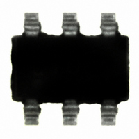
LT1809IS6#TRM Linear Technology, LT1809IS6#TRM Datasheet

LT1809IS6#TRM
Specifications of LT1809IS6#TRM
Available stocks
Related parts for LT1809IS6#TRM
LT1809IS6#TRM Summary of contents
Page 1
... Rail-to-Rail Buffer Amplifi ers n Video Line Driver L, LT, LTC, LTM, Linear Technology and the Linear logo are registered trademarks of Linear Technology Corporation. ThinSOT is a trademark of Linear Technology Corporation. All other trademarks are the property of their respective owners. TYPICAL APPLICATION High Speed ADC Driver ...
Page 2
LT1809/LT1810 ABSOLUTE MAXIMUM RATINGS + – Total Supply Voltage ( ............................. 12.6V Input Voltage (Note 2) ............................................... ±V Input Current (Note 2) ......................................... ±10mA Output Short-Circuit Duration (Note 3) ............ Indefi nite Operating Temperature Range (Note 4) ...
Page 3
ELECTRICAL CHARACTERISTICS unless otherwise noted. SYMBOL PARAMETER V Input Offset Voltage OS ΔV Input Offset Shift OS Input Offset Voltage Match (Channel-to-Channel) (Note 10) I Input Bias Current B ΔI Input Bias Current Shift B Input Bias Current Match (Channel-to-Channel) ...
Page 4
LT1809/LT1810 ELECTRICAL CHARACTERISTICS unless otherwise noted. SYMBOL PARAMETER t Turn-Off Time OFF GBW Gain-Bandwidth Product SR Slew Rate FPBW Full Power Bandwidth THD Total Harmonic Distortion t Settling Time S ΔG Differential Gain (NTSC) Δθ Differential Phase (NTSC) The l ...
Page 5
ELECTRICAL CHARACTERISTICS temperature range 5V, 0V 3V, 0V SYMBOL PARAMETER V Output Voltage Swing HIGH (Note Short-Circuit Current SC I Supply Current per Amplifi Supply Current, Shutdown SHDN ...
Page 6
LT1809/LT1810 ELECTRICAL CHARACTERISTICS temperature range 5V, 0V 3V, 0V SYMBOL PARAMETER CMRR Common Mode Rejection Ratio CMRR Match (Channel-to-Channel) (Note 10) Input Common Mode Range PSRR Power Supply Rejection Ratio PSRR Match (Channel-to-Channel) ...
Page 7
ELECTRICAL CHARACTERISTICS T = 25° ± 5V open, V SHDN SYMBOL PARAMETER ΔI Input Bias Current Shift B Input Bias Current Match (Channel-to-Channel) (Note 10) I Input Offset Current OS ΔI Input Offset ...
Page 8
LT1809/LT1810 ELECTRICAL CHARACTERISTICS temperature range ± 5V open, V SHDN S SYMBOL PARAMETER V Input Offset Voltage Input Offset Voltage Drift (Note 8) OS ΔV Input Offset Voltage Shift OS Input Offset Voltage ...
Page 9
ELECTRICAL CHARACTERISTICS temperature range ±5V open, V SHDN S SYMBOL PARAMETER V Input Offset Voltage Input Offset Voltage Drift (Note 8) OS ΔV Input Offset Voltage Shift OS Input Offset Voltage Match (Channel-to-Channel) ...
Page 10
LT1809/LT1810 ELECTRICAL CHARACTERISTICS Note 1: Stresses beyond those listed under Absolute Maximum Ratings may cause permanent damage to the device. Exposure to any Absolute Maximum Rating condition for extended periods may affect device reliability and lifetime. Note 2: The inputs ...
Page 11
TYPICAL PERFORMANCE CHARACTERISTICS V Distribution (PNP Stage 5V –3 – –2 INPUT OFFSET VOLTAGE (mV) 1809 G01 Supply Current vs Supply Voltage ...
Page 12
LT1809/LT1810 TYPICAL PERFORMANCE CHARACTERISTICS Minimum Supply Voltage 1 V– + 0.5V CM 0.8 0.6 0.4 0 –55° 125°C A –0.2 –0 25°C A –0.6 –0.8 –1.0 1.5 2.0 2.5 3.0 ...
Page 13
TYPICAL PERFORMANCE CHARACTERISTICS Input Noise Voltage vs Frequency 100 NPN ACTIVE 4. PNP ACTIVE 2. 0 FREQUENCY ...
Page 14
LT1809/LT1810 TYPICAL PERFORMANCE CHARACTERISTICS Output Impedance vs Frequency 600 100 0.1 0.01 100k 1M 10M 100M 500M FREQUENCY (Hz) 1809 G28 ...
Page 15
TYPICAL PERFORMANCE CHARACTERISTICS Distortion vs Frequency – P-P – – 100Ω, 2ND L –70 – 1k, 2ND L –90 –100 –110 0.3 1 FREQUENCY ...
Page 16
LT1809/LT1810 APPLICATIONS INFORMATION Rail-to-Rail Characteristics The LT1809/LT1810 have an input and output signal range that includes both negative and positive power supply. Figure 1 depicts a simplifi ed schematic of the amplifi er. The input stage is comprised of two ...
Page 17
APPLICATIONS INFORMATION Table 1. LT1809 6-Lead SOT-23 Package COPPER AREA BOARD AREA 2 2 TOPSIDE (mm ) (mm ) 270 2500 100 2500 20 2500 0 2500 Device is mounted on topside. Table 2. LT1809/LT1810 SO-8 Package COPPER AREA TOPSIDE ...
Page 18
LT1809/LT1810 APPLICATIONS INFORMATION The output of the amplifi er has reverse-biased diodes connected to each supply. If the output is forced beyond either supply, unlimited current will fl ow through these diodes. If the current is transient and limited to ...
Page 19
TYPICAL APPLICATIONS Driving A/D Converters The LT1809/LT1810 have a 27ns settling time to 0. step signal and 20Ω output impedance at 100MHz making it ideal for driving high speed A/D converters. With the rail-to-rail input and output ...
Page 20
LT1809/LT1810 TYPICAL APPLICATIONS P-P 49.9Ω LT1809 2 1 – 4 470pF 1k 1k 0.15μF Figure 6. Single Supply A/D Driver 33μ ...
Page 21
PACKAGE DESCRIPTION 5.23 (.206) MIN 0.42 ± 0.038 (.0165 ± .0015) TYP RECOMMENDED SOLDER PAD LAYOUT 0.254 (.010) GAUGE PLANE 0.18 (.007) NOTE: 1. DIMENSIONS IN MILLIMETER/(INCH) 2. DRAWING NOT TO SCALE 3. DIMENSION DOES NOT INCLUDE MOLD FLASH, PROTRUSIONS ...
Page 22
LT1809/LT1810 PACKAGE DESCRIPTION 0.62 0.95 MAX REF 3.85 MAX 2.62 REF RECOMMENDED SOLDER PAD LAYOUT PER IPC CALCULATOR 0.20 BSC DATUM ‘A’ 0.30 – 0.50 REF NOTE: 1. DIMENSIONS ARE IN MILLIMETERS 2. DRAWING NOT TO SCALE 3. DIMENSIONS ARE ...
Page 23
... MOLD FLASH OR PROTRUSIONS SHALL NOT EXCEED .006" (0.15mm) Information furnished by Linear Technology Corporation is believed to be accurate and reliable. However, no responsibility is assumed for its use. Linear Technology Corporation makes no representa- tion that the interconnection of its circuits as described herein will not infringe on existing patent rights. ...
Page 24
... P-P 274Ω 22pF – 1/2 LT1810 V OUT + 1809 F10 , 70mA Output Current, OS(MAX) , 70mA Output Current, OS(MAX) , Low Noise 3.5nV/√Hz, OS(MAX) LT 0709 REV A • PRINTED IN USA © LINEAR TECHNOLOGY CORPORATION 2000 180910fa ...


