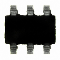
LT1809IS6#TRM Linear Technology, LT1809IS6#TRM Datasheet - Page 10

LT1809IS6#TRM
Manufacturer Part Number
LT1809IS6#TRM
Description
IC OPAMP R-R IN/OUT SNGL SOT23-6
Manufacturer
Linear Technology
Datasheet
1.LT1809CS6TRMPBF.pdf
(24 pages)
Specifications of LT1809IS6#TRM
Amplifier Type
General Purpose
Number Of Circuits
1
Output Type
Rail-to-Rail
Slew Rate
350 V/µs
Gain Bandwidth Product
180MHz
-3db Bandwidth
320MHz
Current - Input Bias
12.5µA
Voltage - Input Offset
800µV
Current - Supply
15mA
Current - Output / Channel
85mA
Voltage - Supply, Single/dual (±)
2.5 V ~ 12.6 V, ±1.25 V ~ 6.3 V
Operating Temperature
-40°C ~ 85°C
Mounting Type
Surface Mount
Package / Case
SOT-23-6
Lead Free Status / RoHS Status
Contains lead / RoHS non-compliant
Other names
LT1809IS6#TRMTR
Available stocks
Company
Part Number
Manufacturer
Quantity
Price
LT1809/LT1810
ELECTRICAL CHARACTERISTICS
Note 1: Stresses beyond those listed under Absolute Maximum Ratings
may cause permanent damage to the device. Exposure to any Absolute
Maximum Rating condition for extended periods may affect device
reliability and lifetime.
Note 2: The inputs are protected by back-to-back diodes. If the differential
input voltage exceeds 1.4V, the input current should be limited to less than
10mA.
Note 3: A heat sink may be required to keep the junction temperature
below the absolute maximum rating when the output is shorted
indefi nitely.
Note 4: The LT1809C/LT1809I and LT1810C/LT1810I are guaranteed
functional over the operating temperature range of – 40°C and 85°C.
Note 5: The LT1809C/LT1810C are guaranteed to meet specifi ed
performance from 0°C to 70°C. The LT1809C/LT1810C are designed,
characterized and expected to meet specifi ed performance from –40°C
to 85°C but are not tested or QA sampled at these temperatures. The
LT1809I/LT1810I are guaranteed to meet specifi ed performance from
–40°C to 85°C.
10
Note 6: Minimum supply voltage is guaranteed by power supply rejection
ratio test.
Note 7: Output voltage swings are measured between the output and
power supply rails.
Note 8: This parameter is not 100% tested.
Note 9: Thermal resistance varies depending upon the amount of PC board
metal attached to the V
amount of 2oz of copper metal trace connecting to the V
in the thermal resistance tables in the Applications Information section.
Note 10: Matching parameters are the difference between the two
amplifi ers of the LT1810.
–
pin of the device. θ
JA
is specifi ed for a certain
–
pin as described
180910fa


