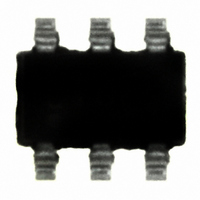
LT1809IS6#TRM Linear Technology, LT1809IS6#TRM Datasheet - Page 16

LT1809IS6#TRM
Manufacturer Part Number
LT1809IS6#TRM
Description
IC OPAMP R-R IN/OUT SNGL SOT23-6
Manufacturer
Linear Technology
Datasheet
1.LT1809CS6TRMPBF.pdf
(24 pages)
Specifications of LT1809IS6#TRM
Amplifier Type
General Purpose
Number Of Circuits
1
Output Type
Rail-to-Rail
Slew Rate
350 V/µs
Gain Bandwidth Product
180MHz
-3db Bandwidth
320MHz
Current - Input Bias
12.5µA
Voltage - Input Offset
800µV
Current - Supply
15mA
Current - Output / Channel
85mA
Voltage - Supply, Single/dual (±)
2.5 V ~ 12.6 V, ±1.25 V ~ 6.3 V
Operating Temperature
-40°C ~ 85°C
Mounting Type
Surface Mount
Package / Case
SOT-23-6
Lead Free Status / RoHS Status
Contains lead / RoHS non-compliant
Other names
LT1809IS6#TRMTR
Available stocks
Company
Part Number
Manufacturer
Quantity
Price
APPLICATIONS INFORMATION
LT1809/LT1810
Rail-to-Rail Characteristics
The LT1809/LT1810 have an input and output signal range
that includes both negative and positive power supply.
Figure 1 depicts a simplifi ed schematic of the amplifi er.
The input stage is comprised of two differential amplifi ers,
a PNP stage Q1/Q2 and a NPN stage Q3/Q4 that are active
over different ranges of common mode input voltage. The
PNP differential pair is active for common mode voltages
between the negative supply to approximately 1.5V below
the positive supply. As the input voltage moves closer
toward the positive supply, the transistor Q5 will steer
the tail current I
the NPN differential pair and causing the PNP pair to
become inactive for the rest of the input common mode
range up to the positive supply.
A pair of complementary common emitter stages
Q14/Q15 form the output stage, enabling the output to
swing from rail-to-rail. The capacitors C1 and C2 form
the local feedback loops that lower the output impedance
at high frequency. These devices are fabricated on Linear
Technology’s proprietary high speed complementary
bipolar process.
16
SHDN
V
V
–
+
V
V
+
–
ESDD5
ESDD6
D9
R6
10k
1
to the current mirror Q6/Q7, activating
R7
100k
Q16
GENERATION
BIAS
Q17
+IN
–IN
V
V
+
–
D6
D5
ESDD1
ESDD4
Figure 1. LT1809 Simplifi ed Schematic Diagram
V
V
+
–
ESDD2
D8
D7
ESDD3
Q4
Q7
D1
D2
Q3
Power Dissipation
The LT1809/LT1810 amplifi ers combine high speed with
large output current in a small package, so there is a need
to ensure that the die’s junction temperature does not
exceed 150°C. The LT1809 is housed in an SO-8 package
or a 6-lead SOT-23 package and the LT1810 is in an SO-8
or 8-lead MSOP package. All packages have the V
ply pin fused to the lead frame to enhance the thermal
conductance when connecting to a ground plane or a large
metal trace. Metal trace and plated through-holes can be
used to spread the heat generated by the device to the
backside of the PC board. For example, on a 3/32" FR-4
board with 2oz copper, a total of 660 square millimeters
connected to Pin 4 of LT1810 in an SO-8 package (330
square millimeters on each side of the PC board) will bring
the thermal resistance, θ
extra metal trace connected to the V
sink, the thermal resistance will be around 105°C/W. More
information on thermal resistance for all packages with
various metal areas connecting to the V
in Tables 1, 2 and 3 for thermal consideration.
Q5
Q6
V
BIAS
Q1
D3
D4
Q2
I
1
Q10
Q11
Q9
R3
R1
JA
Q12
, to about 85°C/W. Without
Q8
R4
R2
C
C
–
pin to provide a heat
V
OUTPUT BIAS
Q13
–
R5
BUFFER
I
–
2
AND
pin is provided
C2
C1
1809 F01
–
Q15
Q14
180910fa
sup-
OUT


