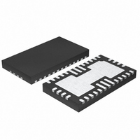
LT6604CUFF-5#PBF Linear Technology, LT6604CUFF-5#PBF Datasheet - Page 11

LT6604CUFF-5#PBF
Manufacturer Part Number
LT6604CUFF-5#PBF
Description
IC AMP DIFF LN DUAL 34-QFN
Manufacturer
Linear Technology
Specifications of LT6604CUFF-5#PBF
Amplifier Type
Differential
Number Of Circuits
2
Output Type
Differential
Current - Input Bias
30µA
Voltage - Input Offset
8000µV
Current - Supply
30mA
Voltage - Supply, Single/dual (±)
3 V ~ 11 V, ±1.5 V ~ 5.5 V
Operating Temperature
0°C ~ 70°C
Mounting Type
Surface Mount
Package / Case
34-QFN
No. Of Amplifiers
2
Input Offset Voltage
35mV
Bandwidth
5MHz
Supply Voltage Range
3V To 11V
Supply Current
30mA
Amplifier Case Style
QFN
No. Of Pins
34
Rohs Compliant
Yes
Lead Free Status / RoHS Status
Lead free / RoHS Compliant
Current - Output / Channel
-
-3db Bandwidth
-
Slew Rate
-
Gain Bandwidth Product
-
Available stocks
Company
Part Number
Manufacturer
Quantity
Price
APPLICATIONS INFORMATION
The two amplifi ers inside the LT6604-5 channel have in-
dependent control of their output common mode voltage
(see the Block Diagram section). The following guidelines
will optimize the performance of the fi lter.
V
AC ground with a 0.01μF capacitor or some instability may
be observed. V
source, provided it remains at least 1.5V above V
least 1.5V below V
voltage of V
matched, their absolute value can vary by ±20%. This
should be taken into consideration when connecting an
external resistor network to alter the voltage of V
V
common mode output voltage is required, connect V
to a voltage source or resistor network. For 3V and 3.3V
supplies the voltage at V
to the mid supply level. For example, voltage (V
1.65V on a single 3.3V supply. For power supply voltages
higher than 3.3V the voltage at V
supply. The voltage on V
below the voltage on V
not be more than 2V above the voltage on V
a high impedance input.
MID
OCM
can be allowed to fl oat, but it must be bypassed to an
can be shorted to V
–100
–120
–20
–40
–60
–80
20
0
MID
Figure 6. Differential Voltage Range
0
COMPRESSION POINTS
1dB PASSBAND GAIN
MID
. While the internal 11k resistors are well
1
+
3RD HARMONIC
T
can be driven from a low impedance
A
. An internal resistor divider sets the
1MHz INPUT LEVEL (V
= 25°C
2
MID
OCM
OCM
3
MID
. The voltage on V
3RD HARMONIC
T
2ND HARMONIC
T
A
A
= 85°C
should not be more than 1V
= 25°C, GAIN = 1
must be less than or equal
4
for simplicity. If a different
OCM
2ND HARMONIC
T
1MHz T
1MHz T
A
5
= 85°C
P-P
can be set above mid
)
A
A
= 25°C
= 85°C
6
6600 F06
7
MID
OCM
. V
–
MID
OCM
should
OCM
and at
.
OCM
) ≤
is
The LT6604-5 was designed to process a variety of input
signals including signals centered on the mid supply
voltage and signals that swing between ground and a
positive voltage in a single supply system (Figure 1). The
allowable range of the input common mode voltage (the
average of V
the power supply level and gain setting (see the Electrical
Characteristics section).
Common Mode DC Currents
In applications like Figure 1 and Figure 3 where the LT6604-5
not only provides lowpass fi ltering but also level shifts the
common mode voltage of the input signal, DC currents
will be generated through the DC path between input and
output terminals. Minimize these currents to decrease
power dissipation and distortion.
Consider the application in Figure 3. V
common mode voltage of the 1st differential amplifi er
inside the LT6604-5 (see the Block Diagram section) at
2.5V. Since the input common mode voltage is near 0V,
there will be approximately a total of 2.5V drop across the
series combination of the internal 806Ω feedback resistor
and the external 200Ω input resistor. The resulting 2.5mA
common mode DC current in each input path, must be
absorbed by the sources V
common mode output voltage of the 2nd differential
amplifi er inside the LT6604-5 channel, and therefore sets
the common mode output voltage of the fi lter. Since, in
the example of Figure 3, V
an additional 1.25mA (625μA per side) of DC current will
fl ow in the resistors coupling the 1st differential amplifi er
output stage to the fi lter output. Thus, a total of 6.25mA
is used to translate the common mode voltages.
A simple modifi cation to Figure 3 will reduce the DC com-
mon mode currents by 36%. If V
common mode output voltage of both op amp stages will
be 2V and the resulting DC current will be 4mA. Of course,
by AC coupling the inputs of Figure 3 and shorting V
V
OCM
, the common mode DC current is eliminated.
IN
+
and V
IN
–
OCM
in Figure 1) is determined by
IN
+
differs from V
MID
and V
is shorted to V
IN
MID
LT6604-5
–
. V
sets the output
OCM
MID
sets the
by 0.5V,
OCM
11
MID
66045fa
the
to


