LT6604CUFF-5#PBF Linear Technology, LT6604CUFF-5#PBF Datasheet - Page 7
LT6604CUFF-5#PBF
Manufacturer Part Number
LT6604CUFF-5#PBF
Description
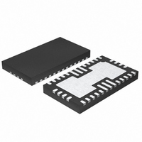
IC AMP DIFF LN DUAL 34-QFN
Manufacturer
Linear Technology
Specifications of LT6604CUFF-5#PBF
Amplifier Type
Differential
Number Of Circuits
2
Output Type
Differential
Current - Input Bias
30µA
Voltage - Input Offset
8000µV
Current - Supply
30mA
Voltage - Supply, Single/dual (±)
3 V ~ 11 V, ±1.5 V ~ 5.5 V
Operating Temperature
0°C ~ 70°C
Mounting Type
Surface Mount
Package / Case
34-QFN
No. Of Amplifiers
2
Input Offset Voltage
35mV
Bandwidth
5MHz
Supply Voltage Range
3V To 11V
Supply Current
30mA
Amplifier Case Style
QFN
No. Of Pins
34
Rohs Compliant
Yes
Lead Free Status / RoHS Status
Lead free / RoHS Compliant
Current - Output / Channel
-
-3db Bandwidth
-
Slew Rate
-
Gain Bandwidth Product
-
Available stocks
Company
Part Number
Manufacturer
Quantity
Price


TYPICAL PERFORMANCE CHARACTERISTICS
+INA, –INA (Pins 2, 4): Channel A Input Pins. Signals can
be applied to either or both input pins through identical
external resistors, R
inputs to the differential outputs is 806Ω/R
V
for the 2nd Filter Stage in channel A. Its value programs
the common mode voltage of the differential output of
the fi lter. Pin 6 is a high impedance input, which can be
driven from an external voltage reference, or Pin 6 can be
tied to Pin 34 on the PC board. Pin 6 should be bypassed
with a 0.01μF ceramic capacitor unless it is connected to
a ground plane.
V
Can be ground.
V
supply, see Block Diagram. For single supply operation
the V
ceramic capacitor to V
can be bypassed or connected to a high quality DC ground.
A ground plane should be used. A poor ground will increase
noise and distortion. Pin 8 sets the output common mode
voltage of the 1st stage of the fi lter in channel B. It has a
5.5kΩ impedance, and it can be overridden with an external
low impedance voltage source.
PIN FUNCTIONS
OCMA
–
MIDB
(Pins 7, 24, 31, 32, 35): Negative Power Supply Pin.
MIDB
(Pin 8): The V
(Pin 6): DC Common Mode Reference Voltage
pin should be bypassed with a quality 0.01μF
45
40
35
30
25
20
15
10
5
0
0.01
Input Referred Noise
IN
MIDB
. The DC gain from the differential
–
. For dual supply operation, Pin 8
INTEGRATED NOISE, GAIN = 1X
INTEGRATED NOISE, GAIN = 4X
NOISE DENSITY, GAIN = 1X
NOISE DENSITY, GAIN = 4X
0.1
pin is internally biased at mid
FREQUENCY (MHz)
1
10
IN
66045 G17
.
100
90
80
70
60
50
40
30
20
10
0
+INB, –INB (Pins 10, 12): Channel B Input Pins. Signals
can be applied to either or both input pins through identi-
cal external resistors, R
inputs to the differential outputs is 806Ω/R
V
for the 2nd Filter Stage in Channel B. Its value programs
the common mode voltage of the differential output of
the fi lter. Pin 14 is a high impedance input, which can be
driven from an external voltage reference, or Pin 14 can be
tied to Pin 8 on the PC board. Pin 14 should be bypassed
with a 0.01μF ceramic or greater capacitor unless it is
connected to a ground plane.
V
for Channels A and B. For a single 3.3V or 5V supply
(V
is required from each positive supply pin (V
the negative supply pin (V
close as possible to the IC. For dual supply applications,
bypass the negative supply pins to ground and each of the
positive supply pins (V
0.1μF ceramic capacitor.
+OUTB, –OUTB (Pins 19, 21): Output Pins. Pins 19 and
21 are the fi lter differential outputs for channel B. With a
typical short-circuit current limit greater than ±40mA, each
pin can drive a 100Ω and/or 50pF load to AC ground.
OCMB
+
–
A, V
–110
–130
grounded) a quality 0.1μF ceramic bypass capacitor
–10
–30
–50
–70
–90
100k
+
(Pin 14): DC Common Mode Reference Voltage
Channel Separation
vs Frequency (Note 9)
V
V
R
EACH OUTPUT
GAIN = 1
B (Pins 25, 17): Positive Power Supply Pins
IN
S
L
= 5V
= 800Ω AT
= 2V
P-P
1M
FREQUENCY (Hz)
+
IN
A, V
10M
. The DC gain from differential
–
). The bypass should be as
+
B) to ground with a quality
66045 G18
100M
LT6604-5
IN
.
+
A, V
+
B) to
66045fa
7
Related parts for LT6604CUFF-5#PBF
Image
Part Number
Description
Manufacturer
Datasheet
Request
R

Part Number:
Description:
IC AMP DIFF LN DUAL 34-QFN
Manufacturer:
Linear Technology
Datasheet:
Part Number:
Description:
IC AMP DIFF LN DUAL 34-QFN
Manufacturer:
Linear Technology
Datasheet:
Part Number:
Description:
IC AMP DIFF LN DUAL 34-QFN
Manufacturer:
Linear Technology
Datasheet:
Part Number:
Description:
IC AMP DIFF LN DUAL 34-QFN
Manufacturer:
Linear Technology
Datasheet:
Part Number:
Description:
IC AMP DIFF LN DUAL 34-QFN
Manufacturer:
Linear Technology
Datasheet:
Part Number:
Description:
IC AMP DIFF LN DUAL 34-QFN
Manufacturer:
Linear Technology
Datasheet:
Part Number:
Description:
IC AMP DIFF LN DUAL 34-QFN
Manufacturer:
Linear Technology
Datasheet:

Part Number:
Description:
Dual Very Low Noise, Differential Amplifi er and 2.5MHz Lowpass Filter
Manufacturer:
LINER [Linear Technology]
Datasheet:
Part Number:
Description:
Dual Very Low Noise, Differential Amplifi er and 5MHz Lowpass Filter
Manufacturer:
LINER [Linear Technology]
Datasheet:

Part Number:
Description:
CD ROM LINEARVIEW DATASHEETS
Manufacturer:
Linear Technology

Part Number:
Description:
Standalone Linear Li-Ion Battery Charger with Thermal Regulation in ThinSOT
Manufacturer:
Linear Technology Corporation
Datasheet:
Part Number:
Description:
Low noise, high frequency, 8th order linear phase lowpass filter
Manufacturer:
Linear Technology Corporation
Datasheet:
Part Number:
Description:
Manufacturer:
Linear Technology Corporation
Datasheet:
Part Number:
Description:
Manufacturer:
Linear Technology Corporation
Datasheet:
Part Number:
Description:
Manufacturer:
Linear Technology Corporation
Datasheet: