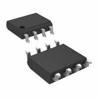
LMH6619MA/NOPB National Semiconductor, LMH6619MA/NOPB Datasheet - Page 25

LMH6619MA/NOPB
Manufacturer Part Number
LMH6619MA/NOPB
Description
IC AMP DUAL RRIO 130MHZ 8-SOIC
Manufacturer
National Semiconductor
Series
PowerWise®r
Specifications of LMH6619MA/NOPB
Amplifier Type
Voltage Feedback
Number Of Circuits
2
Output Type
Rail-to-Rail
Slew Rate
57 V/µs
Gain Bandwidth Product
58MHz
-3db Bandwidth
140MHz
Current - Input Bias
1.5µA
Voltage - Input Offset
100µV
Current - Supply
1.45mA
Current - Output / Channel
35mA
Voltage - Supply, Single/dual (±)
2.7 V ~ 11 V, ±1.35 V ~ 5.5 V
Operating Temperature
-40°C ~ 125°C
Mounting Type
Surface Mount
Package / Case
8-SOIC (3.9mm Width)
Bandwidth
130 MHz
Common Mode Rejection Ratio
96
Current, Input Bias
1 μA (NPN Active), -1.5 μA (PNP Active)
Current, Input Offset
0.01 μA
Current, Output
±35 mA
Current, Supply
1.3 mA
Impedance, Thermal
160 °C/W
Number Of Amplifiers
Dual
Package Type
SOIC-8
Resistance, Input
8 Megohms
Temperature, Operating, Range
-40 to +125 °C
Time, Fall
30 ns
Time, Rise
30 ns
Voltage, Gain
100 dB
Voltage, Input
2.7 to 11 V
Voltage, Noise
10 nV/sqrt Hz
Voltage, Offset
0.1 mV
Voltage, Output, High
230 mV
Voltage, Output, Low
255 mV
Voltage, Supply
5 V
Number Of Channels
2
Voltage Gain Db
100 dB
Common Mode Rejection Ratio (min)
81 dB
Input Offset Voltage
0.6 mV at 5 V
Operating Supply Voltage
3 V, 5 V, 9 V
Supply Current
3 mA at 5 V
Maximum Operating Temperature
+ 125 C
Minimum Operating Temperature
- 40 C
For Use With
551600075-001 - BOARD FOR SOIC LMH6612/19551600074-001 - BOARD FOR SOIC LMH6612/19
Lead Free Status / RoHS Status
Lead free / RoHS Compliant
Other names
LMH6619MA
Note:
GBWP = 65 MHz
C
C
V
Figure 12 shows the frequency response for the various pho-
todiodes in Table 3.
FIGURE 12. Frequency Response for Various Photodiode
When analyzing the noise at the output of the TIA, it is im-
portant to note that the various noise sources (i.e. op amp
S
T
IN
= C
= ±2.5V
= 2 pF
PD
(pF)
C
100
222
22
47
+ C
PD
IN
and Feedback Capacitors
(pF)
102
224
C
24
49
T
TABLE 3. TIA (Figure 1) Compensation and Performance Results
C
10.9
15.8
23.4
(pF)
F CAL
7.7
20195868
C
F USED
(pF)
5.6
10
15
18
25
noise voltage, feedback resistor thermal noise, input noise
current, photodiode noise current) do not all operate over the
same frequency band. Therefore, when the noise at the out-
put is calculated, this should be taken into account. The op
amp noise voltage will be gained up in the region between the
noise gain’s zero and pole (f
the values of R
starts and therefore its contribution to the total output noise
will be larger. It is obvious to note that it is advantageous to
minimize C
reverse bias across the diode at the expense of excess dark
current and noise.
DIFFERENTIAL CABLE DRIVER FOR NTSC VIDEO
The LMH6618 and LMH6619 can be used to drive an NTSC
video signal on a twisted-pair cable. Figure 13 shows the
schematic of a differential cable driver for NTSC video. This
circuit can be used to transmit the signal from a camera over
a twisted pair to a monitor or display located a distance. C
and C
LMH6619. The two amplifiers of the LMH6619 are set to a
gain of 2 to compensate for the 75Ω back termination resistors
on the outputs. The LMH6618 is set to a gain of 1. Because
of the DC bias the output of the LMH6618 is AC coupled. Most
monitors and displays will accept AC coupled inputs.
2
are used to AC couple the video signal into the
f
−3 dB CAL
(MHz)
IN
23.7
16.6
11.5
7.81
by proper choice of op amp or by applying a
F
and C
T
, the sooner the noise gain peaking
f
Z
−3 dB MEAS
and f
(MHz)
15.2
10.8
20
8
P
in Figure 11). The higher
Peaking
www.national.com
(dB)
0.9
0.8
0.9
2.9
1


