LF412ACN/NOPB National Semiconductor, LF412ACN/NOPB Datasheet

IC OP AMP DUAL LOW JFET IN 8-DIP

LF412ACN/NOPB

Manufacturer Part Number
LF412ACN/NOPB
Description
IC OP AMP DUAL LOW JFET IN 8-DIP
Manufacturer
National Semiconductor
Series
BI-FET II™r
Type
General Purpose Amplifierr
Datasheets

Specifications of LF412ACN/NOPB

Amplifier Type
J-FET
Number Of Circuits
2
Slew Rate
15 V/µs
Gain Bandwidth Product
4MHz
Current - Input Bias
50pA
Voltage - Input Offset
500µV
Current - Supply
3.6mA
Voltage - Supply, Single/dual (±)
10 V ~ 44 V, ±5 V ~ 22 V
Operating Temperature
0°C ~ 70°C
Mounting Type
Through Hole
Package / Case
8-DIP (0.300", 7.62mm)
Bandwidth
4 MHz
Channel Separation
-120
Common Mode Rejection Ratio
100
Current, Input Bias
50 pA
Current, Input Offset
25 pA
Current, Output
25 mA
Current, Supply
3.6 mA
Harmonic Distortion
0.02 %
Impedance, Thermal
152 °C/W
Number Of Amplifiers
Dual
Package Type
DIP-8
Resistance, Input
10^12 Ohms
Temperature, Operating, Range
0 to +70 °C
Voltage, Gain
200 V/mV
Voltage, Input
10 to 45 V
Voltage, Noise
25 nV/sqrt Hz
Voltage, Offset
0.5 mV
Voltage, Output, High
13.5 V
Voltage, Output, Low
-13.5 V
Voltage, Supply
±19 V
Rail/rail I/o Type
No
Number Of Elements
2
Unity Gain Bandwidth Product
4MHz
Input Offset Voltage
1@±20VmV
Input Bias Current
200pA
Single Supply Voltage (typ)
Not RequiredV
Dual Supply Voltage (typ)
±9/±12/±15/±18V
Power Dissipation
670mW
Voltage Gain In Db
106.02dB
Power Supply Rejection Ratio
80dB
Power Supply Requirement
Dual
Shut Down Feature
No
Single Supply Voltage (min)
Not RequiredV
Single Supply Voltage (max)
Not RequiredV
Dual Supply Voltage (min)
±5V
Dual Supply Voltage (max)
±22V
Technology
BiFET
Operating Temp Range
0C to 70C
Operating Temperature Classification
Commercial
Mounting
Through Hole
Pin Count
8
Op Amp Type
High Speed
No. Of Amplifiers
2
Supply Voltage Range
10V To 44V
Amplifier Case Style
DIP
No. Of Pins
8
Operating Temperature Range
0°C To +70°C
Rohs Compliant
Yes
Lead Free Status / RoHS Status
Lead free / RoHS Compliant
Output Type
-
Current - Output / Channel
-
-3db Bandwidth
-
Lead Free Status / Rohs Status
RoHS Compliant part Electrostatic Device
Other names
*LF412ACN
*LF412ACN/NOPB
LF412ACN

Available stocks

Company
Part Number
Manufacturer
Quantity
Price
Part Number:
LF412ACN/NOPB
Manufacturer:
TI
Quantity:
2 000
© 2004 National Semiconductor Corporation
LF412
Low Offset, Low Drift Dual JFET Input Operational
Amplifier
General Description
These devices are low cost, high speed, JFET input opera-
tional amplifiers with very low input offset voltage and guar-
anteed input offset voltage drift. They require low supply
current yet maintain a large gain bandwidth product and fast
slew rate. In addition, well matched high voltage JFET input
devices provide very low input bias and offset currents. The
LF412 dual is pin compatible with the LM1558, allowing
designers to immediately upgrade the overall performance of
existing designs.
These amplifiers may be used in applications such as high
speed integrators, fast D/A converters, sample and hold
circuits and many other circuits requiring low input offset
voltage and drift, low input bias current, high input imped-
ance, high slew rate and wide bandwidth.
Typical Connection
Ordering Information
X indicates electrical grade
Y indicates temperature range
Z indicates package type
BI-FET II
LF412XYZ
“M” for military
“C” for commercial
“H” or “N”
is a trademark of National Semiconductor Corporation.
DS005656
00565641
Features
n Internally trimmed offset voltage:
n Input offset voltage drift: 10 µV/˚C (max)
n Low input bias current: 50 pA
n Low input noise current:
n Wide gain bandwidth: 3 MHz (min)
n High slew rate: 10V/µs (min)
n Low supply current: 1.8 mA/Amplifier
n High input impedance: 10
n Low total harmonic distortion
n Low 1/f noise corner: 50 Hz
n Fast settling time to 0.01%: 2 µs
Connection Diagrams
See NS Package Number J08A or N08E
Order Number LF412ACN, LF412CN
Order Number LF412MH, LF412CH
See NS Package Number H08A
or LF412MH/883 (Note 1)
or LF412MJ/883 (Note 1)
Dual-In-Line Package
Metal Can Package
12
≤0.02%
1 mV (max)
00565642
00565644

Related parts for LF412ACN/NOPB

LF412ACN/NOPB Summary of contents

Page 1

... Z indicates package type “H” or “N” BI-FET II ™ trademark of National Semiconductor Corporation. © 2004 National Semiconductor Corporation Features n Internally trimmed offset voltage: n Input offset voltage drift: 10 µV/˚C (max) n Low input bias current ...

Page 2

... Absolute Maximum Ratings If Military/Aerospace specified devices are required, please contact the National Semiconductor Sales Office/ Distributors for availability and specifications. (Note 11) LF412A ± Supply Voltage ± Differential Input Voltage Input voltage Range ± (Note 3) Output Short Circuit Duration (Note 4) Continuous H Package ...

Page 3

AC Electrical Characteristics (Note 7) Symbol Parameter THD Total Harmonic Dist e Equivalent Input Noise n Voltage i Equivalent Input Noise n Current Note 3: Unless otherwise specified the absolute maximum negative input voltage is equal to the negative power ...

Page 4

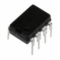
Physical Dimensions inches (millimeters) unless otherwise noted (Continued) Dual-In-Line Package (J) Order Number LF412MJ/883 NS Package Number J08A Dual-In-Line Package (N) Order Number LF412ACN or LF412CN NS Package Number N08E 12 ...

Related keywords