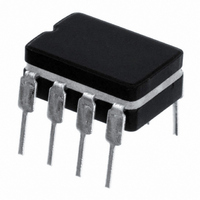
LM158J National Semiconductor, LM158J Datasheet - Page 8

LM158J
Manufacturer Part Number
LM158J
Description
IC OP AMP LOW PWR DUAL 8-CDIP
Manufacturer
National Semiconductor
Specifications of LM158J
Amplifier Type
General Purpose
Number Of Circuits
2
Slew Rate
0.5 V/µs
Gain Bandwidth Product
1MHz
Current - Input Bias
45nA
Voltage - Input Offset
2000µV
Current - Supply
1mA
Current - Output / Channel
40mA
Voltage - Supply, Single/dual (±)
3 V ~ 32 V, ±1.5 V ~ 16 V
Operating Temperature
-55°C ~ 125°C
Mounting Type
Through Hole
Package / Case
8-CDIP (0.300", 7.62mm)
Bandwidth
1 MHz
Channel Separation
-120
Common Mode Rejection Ratio
85
Current, Input Bias
45 nA
Current, Input Offset
3 nA
Current, Output
40 mA
Current, Supply
0.5 mA
Number Of Amplifiers
Dual
Package Type
CDIP-8
Temperature, Operating, Range
-55 to +125 °C
Voltage, Gain
100 V/mV
Voltage, Input
-0.3 to +32 V
Voltage, Offset
2 mV
Voltage, Output, High
28 V
Voltage, Output, Low
5 mV
Voltage, Supply
5 V
Lead Free Status / RoHS Status
Contains lead / RoHS non-compliant
Output Type
-
-3db Bandwidth
-
Other names
*LM158J
Available stocks
Company
Part Number
Manufacturer
Quantity
Price
Company:
Part Number:
LM158J
Manufacturer:
TI/NS
Quantity:
1 000
Company:
Part Number:
LM158J
Manufacturer:
TI/NS
Quantity:
1 000
Part Number:
LM158J
Manufacturer:
SCS
Quantity:
20 000
Company:
Part Number:
LM158J/883
Manufacturer:
TI
Quantity:
5 510
Company:
Part Number:
LM158J/883
Manufacturer:
SIEMENS
Quantity:
5 510
www.national.com
Typical Performance Characteristics
Application Hints
The LM158 series are op amps which operate with only a
single power supply voltage, have true-differential inputs,
and remain in the linear mode with an input common-mode
voltage of 0 V
of power supply voltage with little change in performance
characteristics. At 25˚C amplifier operation is possible down
to a minimum supply voltage of 2.3 V
Precautions should be taken to insure that the power supply
for the integrated circuit never becomes reversed in polarity
or that the unit is not inadvertently installed backwards in a
test socket as an unlimited current surge through the result-
ing forward diode within the IC could cause fusing of the
internal conductors and result in a destroyed unit.
Large differential input voltages can be easily accomodated
and, as input differential voltage protection diodes are not
needed, no large input currents result from large differential
input voltages. The differential input voltage may be larger
than V
provided to prevent the input voltages from going negative
more than −0.3 V
resistor to the IC input terminal can be used.
To reduce the power supply current drain, the amplifiers
have a class A output stage for small signal levels which
converts to class B in a large signal mode. This allows the
amplifiers to both source and sink large output currents.
Therefore both NPN and PNP external current boost transis-
tors can be used to extend the power capability of the basic
amplifiers. The output voltage needs to raise approximately
1 diode drop above ground to bias the on-chip vertical PNP
transistor for output current sinking applications.
For ac applications, where the load is capacitively coupled to
the output of the amplifier, a resistor should be used, from
the output of the amplifier to ground to increase the class A
bias current and prevent crossover distortion. Where the
load is directly coupled, as in dc applications, there is no
crossover distortion.
+
without damaging the device. Protection should be
DC
Input Current (LM2902 only)
. These amplifiers operate over a wide range
DC
(at 25˚C). An input clamp diode with a
DC
.
00778746
8
(Continued)
Capacitive loads which are applied directly to the output of
the amplifier reduce the loop stability margin. Values of 50
pF can be accomodated using the worst-case non-inverting
unity gain connection. Large closed loop gains or resistive
isolation should be used if larger load capacitance must be
driven by the amplifier.
The bias network of the LM158 establishes a drain current
which is independent of the magnitude of the power supply
voltage over the range of 3 V
Output short circuits either to ground or to the positive power
supply should be of short time duration. Units can be de-
stroyed, not as a result of the short circuit current causing
metal fusing, but rather due to the large increase in IC chip
dissipation which will cause eventual failure due to exces-
sive function temperatures. Putting direct short-circuits on
more than one amplifier at a time will increase the total IC
power dissipation to destructive levels, if not properly pro-
tected with external dissipation limiting resistors in series
with the output leads of the amplifiers. The larger value of
output source current which is available at 25˚C provides a
larger output current capability at elevated temperatures
(see typical performance characteristics) than a standard IC
op amp.
The circuits presented in the section on typical applications
emphasize operation on only a single power supply voltage.
If complementary power supplies are available, all of the
standard op amp circuits can be used. In general, introduc-
ing a pseudo-ground (a bias voltage reference of V
allow operation above and below this value in single power
supply systems. Many application circuits are shown which
take advantage of the wide input common-mode voltage
range which includes ground. In most cases, input biasing is
not required and input voltages which range to ground can
easily be accommodated.
Voltage Gain (LM2902 only)
DC
to 30 V
DC
.
00778747
+
/2) will


