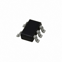
CLC404AJM5 National Semiconductor, CLC404AJM5 Datasheet

CLC404AJM5
Specifications of CLC404AJM5
Related parts for CLC404AJM5
CLC404AJM5 Summary of contents
Page 1
... SMD Number: 5962-90994 Space level versions also available. For more information, visit http://www.national.com/mil Connection Diagrams Pinout DIP & SOIC © 2001 National Semiconductor Corporation Features n 165MHz large signal bandwidth (5V n 2600V/µs slew rate n Low Power: 110mW n Low distortion: −53dBc at 20MHz n 10ns settling to 0.2% n 0.07% diff. gain, 0.03˚ ...
Page 2
... Absolute Maximum Ratings If Military/Aerospace specified devices are required, please contact the National Semiconductor Sales Office/ Distributors for availability and specifications. Supply Voltage ( OUT Output is short circuit protected to ground, but maximum reliability will be maintained if I does not OUT exceed... Common Mode Input Voltage ...
Page 3
... No Load, Quiescent 11 Resistance 1000 Capacitance 0.1 ± No Load ± For Rated Performance ± +2, R 500 ,R 150 1V equivalent video signal, 0-100 IRE, 40 IRE Part Number Industrial CLC404AJP CLC404AJE CLC404AJM5 3 Typ Max/Min Ratings (Note 2) < < < > > > 250 500 1000 < < < < < < ...
Page 4
Typical Performance Characteristics Frequency Response A Frequency Response A Bandwidth vs Load Capacitance www.national.com = +2V/V V 01274601 = +20V/V V 01274603 Recommended R 01274605 4 Frequency Response A = +6V/V V 01274602 Inverting Frequency Response 01274604 vs Load Capacitance ...
Page 5
Typical Performance Characteristics Large Signal Pulse Response 3rd Harmonic Dist. vs. Amplitude 2nd Harmonic Distortion C (Continued) 2nd Harmonic Dist. vs. Amplitude 01274607 01274609 = 25pF 3rd Harmonic Distortion C L 01274611 5 01274608 Settling Time 01274610 = 25pF L ...
Page 6
Typical Performance Characteristics Equivalent Input Noise CMRR and PSRR www.national.com (Continued) Differential Gain and Phase vs. Load 01274613 01274615 6 01274614 ...
Page 7
Application Division FIGURE 1. Recommended Non-Inverting Gain Circuit FIGURE 2. Recommended Inverting Gain Circuit Slew Rate Slew rate limiting is a nonlinear response which occurs in amplifiers when the output voltage swing approaches hard, abrupt limits in the speed at ...
Page 8
Differential Gain and Phase Differential gain and phase are measurements useful prima- rily in composite video channels. Differential gain and phase are measured by monitoring the gain and phase of a high frequency carrier (3.58MHz for NTSC composite video) as ...
Page 9
Physical Dimensions inches (millimeters) unless otherwise noted NS Product Number M08A NS Product Number MA05A 9 www.national.com ...
Page 10
... NATIONAL’S PRODUCTS ARE NOT AUTHORIZED FOR USE AS CRITICAL COMPONENTS IN LIFE SUPPORT DEVICES OR SYSTEMS WITHOUT THE EXPRESS WRITTEN APPROVAL OF THE PRESIDENT AND GENERAL COUNSEL OF NATIONAL SEMICONDUCTOR CORPORATION. As used herein: 1. Life support devices or systems are devices or systems which, (a) are intended for surgical implant ...


