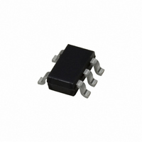
CLC409AJM5 National Semiconductor, CLC409AJM5 Datasheet

CLC409AJM5
Specifications of CLC409AJM5
Available stocks
Related parts for CLC409AJM5
CLC409AJM5 Summary of contents
Page 1
... SMD Number: 5962-92034 Space level versions also available. For more information, visit http://www.national.com/mil Connection Diagrams Pinout DIP & SOIC © 2002 National Semiconductor Corporation Features n 350MHz small signal bandwidth n -65/−72dBc 2nd/3rd harmonics (20MHz) n Low noise n 8ns settling to 0.1% ± ...
Page 2
... Absolute Maximum Ratings If Military/Aerospace specified devices are required, please contact the National Semiconductor Sales Office/ Distributors for availability and specifications. Supply Voltage ( OUT Output is short circuit protected to ground, but maximum reliability will be maintained if I does not OUT exceed... Common Mode Input Voltage ...
Page 3
... DC 0.1 ± 100Ω 3.5 L ± 2.2 60 Part Number Industrial −40˚C to +85˚C CLC409AJP −40˚C to +85˚C CLC409AJE −40˚C to +85˚C CLC409AJM5 3 Max/Min Units (Note 2) < < < 8.5 4.5 9.5 mV < < µV/˚C < < < ...
Page 4
Typical Performance Characteristics Unless Specified). Non-Inverting Frequency Response Frequency Response for Various R Short-Term Settling Response www.national.com (T = 25˚ + Inverting Frequency Response 01274801 S Small Signal Pulse Response L 01274803 Long-Term Settling ...
Page 5
Typical Performance Characteristics Unless Specified). (Continued) Harmonic Distortion vs. Load and Frequency Settling Time vs. Capacitive Load 3rd Harmonic Distortion vs 25˚ + 2-Tone, 3rd Order Spurious Levels 01274804 2nd Harmonic Distortion ...
Page 6
Typical Performance Characteristics Unless Specified). (Continued) Equivalent Input Noise Open-Loop Transimpedance Gain, Z(s) www.national.com (T = 25˚ + PSRR, CMRR, and Closed Loop R 01274809 01274811 6 ± 5V 100Ω, R ...
Page 7
Application Division FIGURE 1. Recommended Non-Inverting Gain Circuit FIGURE 2. Recommended Inverting Gain Circuit Feedback Resistor The CLC409 achieves its excellent pulse and distortion per- formance by using the current feedback topology pioneered by Comlinear Corporation. The loop gain for ...
Page 8
Application Division CLC409 does not show an intercept type performance. (where the relative spurious levels change rate vs. the test tone powers), due to an internal full power bandwidth enhancement circuit that boosts the performance as the ...
Page 9
Physical Dimensions inches (millimeters) unless otherwise noted 8-Pin MDIP NS Package Number N08E 8-Pin SOIC NS Package Number M08A 9 www.national.com ...
Page 10
... NATIONAL’S PRODUCTS ARE NOT AUTHORIZED FOR USE AS CRITICAL COMPONENTS IN LIFE SUPPORT DEVICES OR SYSTEMS WITHOUT THE EXPRESS WRITTEN APPROVAL OF THE PRESIDENT AND GENERAL COUNSEL OF NATIONAL SEMICONDUCTOR CORPORATION. As used herein: 1. Life support devices or systems are devices or systems which, (a) are intended for surgical implant ...


