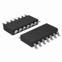
MC33204DG ON Semiconductor, MC33204DG Datasheet - Page 3

MC33204DG
Manufacturer Part Number
MC33204DG
Description
IC OPAMP QUAD R-R LV 14-SOIC
Manufacturer
ON Semiconductor
Datasheet
1.MC33201PG.pdf
(18 pages)
Specifications of MC33204DG
Amplifier Type
General Purpose
Number Of Circuits
4
Output Type
Rail-to-Rail
Slew Rate
1 V/µs
Gain Bandwidth Product
2.2MHz
Current - Input Bias
80nA
Voltage - Input Offset
10000µV
Current - Supply
1.125mA
Current - Output / Channel
80mA
Voltage - Supply, Single/dual (±)
1.8 V ~ 12 V, ±0.9 V ~ 6 V
Operating Temperature
-40°C ~ 105°C
Mounting Type
Surface Mount
Package / Case
14-SOIC (3.9mm Width), 14-SOL
Number Of Channels
4
Common Mode Rejection Ratio (min)
60 dB
Input Voltage Range (max)
Positive Rail
Input Voltage Range (min)
Negative Rail
Input Offset Voltage
10 mV
Input Bias Current (max)
200 nA
Operating Supply Voltage
12 V
Supply Current
3.6 mA
Maximum Operating Temperature
+ 105 C
Minimum Operating Temperature
- 40 C
Dual Supply Voltage
+/- 3 V, +/- 5 V
Maximum Dual Supply Voltage
+/- 6 V
Minimum Dual Supply Voltage
+/- 0.9 V
Mounting Style
SMD/SMT
Shutdown
No
Supply Voltage (max)
12 V
Supply Voltage (min)
1.8 V
Technology
Bipolar
Voltage Gain Db
109.54 dB
Lead Free Status / RoHS Status
Lead free / RoHS Compliant
-3db Bandwidth
-
Lead Free Status / Rohs Status
Lead free / RoHS Compliant
Other names
MC33204DG
MC33204DGOS
MC33204DGOS
Available stocks
Company
Part Number
Manufacturer
Quantity
Price
Company:
Part Number:
MC33204DG
Manufacturer:
ON
Quantity:
5 510
Company:
Part Number:
MC33204DG
Manufacturer:
PHILIPS
Quantity:
5 510
Company:
Part Number:
MC33204DG
Manufacturer:
MOTOROLA
Quantity:
80
Part Number:
MC33204DG
Manufacturer:
ON
Quantity:
20 000
Specifications at V
Stresses exceeding Maximum Ratings may damage the device. Maximum Ratings are stress ratings only. Functional operation above the
Recommended Operating Conditions is not implied. Extended exposure to stresses above the Recommended Operating Conditions may affect
device reliability.
1. The differential input voltage of each amplifier is limited by two internal parallel back−to−back diodes. For additional differential input voltage
2. The input common mode voltage range is limited by internal diodes connected from the inputs to both supply rails. Therefore, the voltage
3. Power dissipation must be considered to ensure maximum junction temperature (T
4. NCV33202 and NCV33204 are qualified for automotive use.
MAXIMUM RATINGS
DC ELECTRICAL CHARACTERISTICS
DC ELECTRICAL CHARACTERISTICS
Supply Voltage (V
Input Differential Voltage Range
Common Mode Input Voltage Range (Note 2)
Output Short Circuit Duration
Maximum Junction Temperature
Storage Temperature
Maximum Power Dissipation
Input Offset Voltage
Output Voltage Swing
Power Supply Current
Input Offset Voltage (V
Input Offset Voltage Temperature Coefficient (R
Input Bias Current (V
range, use current limiting resistors in series with the input pins.
on either input must not exceed either supply rail by more than 500 mV.
V
V
V
per Amplifier (I
MC33201:
MC33201:
MC33201V:
MC33202:
MC33202:
MC33202V:
NCV33202V: T
MC33204:
MC33204:
MC33204V:
NCV33204:
T
T
T
T
T
MC33201
MC33202, NCV33202
MC33204, NCV33204
A
A
A
A
A
IO (max)
OH
OL
= − 40° to +105°C
= − 55° to +125°C
= + 25°C
= − 40° to +105°C
= − 55° to +125°C
(R
(R
L
L
= 10 kW)
= 10 kW)
Characteristic
CC
CC
D
T
T
T
T
T
T
T
T
T
T
A
A
A
A
A
A
A
A
A
A
A
)
= 3.3 V are guaranteed by the 2.0 V and 5.0 V tests. V
= + 25°C
= − 40° to +105°C
= − 55° to +125°C
= + 25°C
= − 40° to +105°C
= − 55° to +125°C
= − 55° to +125°C (Note 4)
= + 25°C
= − 40° to +105°C
= − 55° to +125°C
= − 55° to +125°C
CM
to V
CM
= 0 V to 0.5 V, V
EE
0 V to 0.5 V, V
Characteristic
)
Rating
CM
CM
1.0 V to 5.0 V)
= 1.0 V to 5.0 V)
(T
(V
A
S
CC
= 25°C)
= 50 W)
= + 5.0 V, V
V
CC
1.125
± 8.0
0.10
±10
±12
1.9
= 2.0 V
http://onsemi.com
EE
= Ground, T
3
EE
Figure
5, 6
= GND.
V
3
4
A
CC
= 25°C, unless otherwise noted.)
1.125
± 8.0
3.15
0.15
±10
±12
= 3.3 V
Symbol
J
V
V
) is not exceeded. (See Figure 2)
T
V
P
T
IDR
CM
t
stg
s
DV
S
D
J
Symbol
⎮V
⎮I
IO
IB
IO
/DT
⎮
⎮
Min
−
−
−
−
−
−
−
−
−
−
−
−
−
−
−
−
V
V
− 65 to +150
CC
V
CC
EE
1.125
Note 1
Note 3
Note 3
± 6.0
± 8.0
Value
4.85
0.15
+ 0.5 V to
+150
±10
+13
= 5.0 V
− 0.5 V
Typ
100
2.0
2.0
80
−
−
−
−
−
−
−
−
−
−
−
−
Max
200
250
500
6.0
9.0
8.0
13
11
14
14
10
13
17
17
−
−
V
Unit
V
mV
mA
Unit
mW
sec
max
min
°C
°C
mV/°C
V
V
V
Unit
mV
nA


