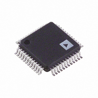
ADM1064ASUZ Analog Devices Inc, ADM1064ASUZ Datasheet - Page 18

ADM1064ASUZ
Manufacturer Part Number
ADM1064ASUZ
Description
IC SEQUENCER/SUPERVISOR 48-TQFP
Manufacturer
Analog Devices Inc
Type
Sequencerr
Datasheet
1.EVAL-ADM1064TQEB.pdf
(32 pages)
Specifications of ADM1064ASUZ
Number Of Voltages Monitored
10
Output
Programmable
Voltage - Threshold
Adjustable/Selectable
Operating Temperature
-40°C ~ 85°C
Mounting Type
Surface Mount
Package / Case
48-TQFP, 48-VQFP
No. Of Supervisors / Monitors
10
Supply Voltage Range
3V To 14.4V
Supply Current
4.2mA
Digital Ic Case Style
TQFP
No. Of Pins
48
Operating Temperature Range
-40°C To +85°C
Svhc
No SVHC
Lead Free Status / RoHS Status
Lead free / RoHS Compliant
For Use With
EVAL-ADM1064LFEBZ - BOARD EVALUATION FOR ADM1064LFEVAL-ADM1064TQEB - BOARD EVALUATION FOR ADM1064TQ
Reset
-
Reset Timeout
-
Lead Free Status / RoHS Status
Lead free / RoHS Compliant, Lead free / RoHS Compliant
Available stocks
Company
Part Number
Manufacturer
Quantity
Price
Company:
Part Number:
ADM1064ASUZ
Manufacturer:
ADI
Quantity:
250
Company:
Part Number:
ADM1064ASUZ
Manufacturer:
Analog Devices Inc
Quantity:
10 000
Part Number:
ADM1064ASUZ
Manufacturer:
ADI/亚德诺
Quantity:
20 000
ADM1064
SEQUENCING ENGINE APPLICATION EXAMPLE
The application in this section demonstrates the operation of
the SE. Figure 25 shows how the simple building block of a single
SE state can be used to build a power-up sequence for a three-
supply system. Table 8 lists the PDOs for each state in the same SE
implementation. In this system, a good 5 V supply on VP1 and
the VX1 pin held low are the triggers required to start a power-up
sequence. The sequence next turns on the 3.3 V supply, then the
2.5 V supply (assuming successful turn-on of the 3.3 V supply).
When all three supplies have turned on correctly, the PWRGD
state is entered, where the SE remains until a fault occurs on one
of the three supplies or until it is instructed to go through a power-
down sequence by VX1 going high.
Faults are dealt with throughout the power-up sequence on
a case-by-case basis. The following three sections (the Sequence
Detector section, the Monitoring Fault Detector section, and
the Timeout Detector section) describe the individual blocks
and use the sample application shown in Figure 25 to demonstrate
the actions of the state machine.
Sequence Detector
The sequence detector block is used to detect when a step in
a sequence is complete. It looks for one of the SE inputs to
change state and is most often used as the gate for successful
progress through a power-up or power-down sequence. A timer
block that is included in this detector can insert delays into a
power-up or power-down sequence, if required. Timer delays
can be set from 10 μs to 400 ms. Figure 24 is a block diagram of
the sequence detector.
Table 8. PDO Outputs for Each State
PDO Outputs
PDO1 = 3V3ON
PDO2 = 2V5ON
PDO3 = FAULT
VP1
VX5
(UNCONDITIONAL JUMP)
LOGIC INPUT CHANGE
OR FAULT DETECTION
SUPPLY FAULT
Figure 24. Sequence Detector Block Diagram
FORCE FLOW
DETECTION
WARNINGS
IDLE1
0
0
0
SELECT
IDLE2
0
0
0
INVERT
SEQUENCE
DETECTOR
EN3V3
1
0
0
TIMER
Rev. C | Page 18 of 32
EN2V5
1
1
0
If a timer delay is specified, the input to the sequence detector
must remain in the defined state for the duration of the timer
delay. If the input changes state during the delay, the timer is reset.
The sequence detector can also help to identify monitoring faults.
In the sample application shown in Figure 25, the FSEL1 and
FSEL2 states first identify which of the VP1,VP2, or VP3 pins
has faulted, and then they take appropriate action.
DIS3V3
0
1
1
VP1 = 0
MONITOR FAULT
FSEL2
VP2) = 0
(VP1 + VP2 + VP3) = 0
Figure 25. Sample Application Flow Diagram
STATES
VP2 = 0
(VP1 +
DIS2V5
1
0
1
(VP1 + VP2) = 0
FSEL1
VP3 = 0
VP1 = 0
SEQUENCE
PWRGD
1
1
0
PWRGD
STATES
EN3V3
EN2V5
IDLE1
IDLE2
VX1 = 0
VP1 = 1
VX1 = 1
VP3 = 1
VP2 = 1
10ms
20ms
VP2 = 0
DIS3V3
DIS2V5
FSEL1
1
1
1
TIMEOUT
STATES
VX1 = 1
VX1 = 1
FSEL2
1
1
1


