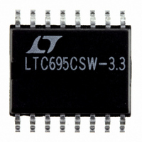
LTC695CSW-3.3 Linear Technology, LTC695CSW-3.3 Datasheet

LTC695CSW-3.3
Specifications of LTC695CSW-3.3
Available stocks
Related parts for LTC695CSW-3.3
LTC695CSW-3.3 Summary of contents
Page 1
... Critical μP Power Monitoring n Intelligent Instruments n Battery-Powered Computers and Controllers n Automotive Systems L, LT, LTC, LTM, Linear Technology and the Linear logo are registered trademarks of Linear Technology Corporation. All other trademarks are the property of their respective owners. TYPICAL APPLICATION LT1129-3.3 V ≥ 3.3V ...
Page 2
LTC694-3.3/LTC695-3.3 ABSOLUTE MAXIMUM RATINGS Terminal Voltage V .......................................................... –0. ...................................................... –0. BATT All Other Inputs ..................... –0. Input Current V ..................................................................100mA CC .................................................................25mA V BATT GND ...................................................................10mA PIN CONFIGURATION TOP VIEW V ...
Page 3
... LTC1232 8 4.37/4.62 LTC1235 16 4.65 LTC694-3.3/LTC695-3.3 PART MARKING PACKAGE DESCRIPTION LTC695CN-3.3 16-Lead PDIP LTC695IN-3.3 16-Lead PDIP LTC695CSW-3.3 16-Lead Plastic Wide SO LTC695ISW-3.3 16-Lead Plastic Wide SO LTC694CN8-3.3 8-Lead PDIP LTC694IN8-3.3 8-Lead PDIP 6943 8-Lead Plastic SO 694I3 8-Lead Plastic SO http://www.linear.com/leadfree/ http://www.linear.com/tapeandreel/ WATCHDOG ...
Page 4
LTC694-3.3/LTC695-3.3 ELECTRICAL CHARACTERISTICS temperature range, otherwise specifications are at T PARAMETER Battery Back-Up Switching Operating Voltage Range V Output Voltage OUT V in Battery Back-Up Mode OUT Supply Current (Exclude I ) OUT Supply Current in Battery Back-Up Mode Battery ...
Page 5
ELECTRICAL CHARACTERISTICS temperature range, otherwise specifications are at T PARAMETER Power-Fail Detector PFI Input Threshold PFI Input Threshold PSRR PFI Input Current PFO Output Voltage (Note 4) PFO Short-Circuit Source Current (Note 4) PFI Comparator Response Time (Falling) PFI Comparator ...
Page 6
LTC694-3.3/LTC695-3.3 TYPICAL PERFORMANCE CHARACTERISTICS Output Voltage vs Load Current 3. 3. 2.4V BATT ° 3. 3.20 SLOPE = 4.6Ω 3.15 3.10 3.05 3. LOAD CURRENT ...
Page 7
PIN FUNCTIONS BATT ON: Battery On Logic Output from Comparator C2. BATT ON goes low when V is internally connected to OUT V . The output typically sinks 25mA and can provide CC base drive for an external PNP transistor ...
Page 8
LTC694-3.3/LTC695-3.3 PIN FUNCTIONS WDI: Watchdog Input. WDI is a three-level input. Driving WDI either high or low for longer than the watchdog timeout period, forces both RESET and WDO low. Floating WDI disables the watchdog timer. The timer resets itself ...
Page 9
APPLICATIONS INFORMATION Microprocessor Reset The LTC694-3.3/LTC695-3.3 use a bandgap voltage refer- ence and a precision voltage comparator C1 to monitor the 3.3V supply input on V (see the Block Diagram). When CC falls below the reset voltage threshold, the RESET ...
Page 10
LTC694-3.3/LTC695-3.3 APPLICATIONS INFORMATION ANY PNP POWER TRANSISTOR 5 BATT 3. OUT 0.1μF LTC695-3 BATT GND 2.4V 4 Figure 2. Using BATT ON to Drive External PNP Transistor The LTC694-3.3/LTC695-3.3 are protected for ...
Page 11
APPLICATIONS INFORMATION If battery connections are made through long wires, a 10Ω to 100Ω series resistor and a 0.1μF capacitor are recommended to prevent any overshoot beyond V to the lead inductance (Figure 4). Table 1 shows the state of ...
Page 12
LTC694-3.3/LTC695-3.3 APPLICATIONS INFORMATION 3. OUT + 0.1μF 10μF LTC695-3.3 CE OUT 30ns PROPAGATION DELAY V BATT CE IN FROM DECODER RESET 2.4V RESET GND TO μP Figure 6. A Typical Nonvolatile CMOS RAM Application V V 3.3V ...
Page 13
APPLICATIONS INFORMATION Example 1: The circuit in Figure 8 demonstrates the use of the power-fail comparator to monitor the unregulated power supply input. Assuming the the rate of decay of the supply input V is 100mV/ms and the total time ...
Page 14
LTC694-3.3/LTC695-3.3 APPLICATIONS INFORMATION V = 3.3V CC WDI WDO RESET t 1 Figure 11. Watchdog Timeout Period and Reset Active Time EXTERNAL CLOCK 3 OSC SEL 3. LTC695-3.3 4 GND INTERNAL OSCILLATOR 1.6 SECOND WATCHDOG 3 V 3.3V ...
Page 15
TYPICAL APPLICATION Table 2. LTC695-3.3 Reset Active Time and Watchdog Timeout Selections OSC SEL OSC IN Low External Clock Input Low External Capacitor* Floating or High Low Floating or High Floating or High *The nominal internal frequency is 10.24kHz. The ...
Page 16
LTC694-3.3/LTC695-3.3 PACKAGE DESCRIPTION .300 – .325 (7.620 – 8.255) .065 (1.651) .008 – .015 TYP (0.203 – 0.381) +.035 .325 –.015 +0.889 8.255 –0.381 NOTE: INCHES 1. DIMENSIONS ARE MILLIMETERS *THESE DIMENSIONS DO NOT INCLUDE MOLD FLASH OR PROTRUSIONS. MOLD ...
Page 17
PACKAGE DESCRIPTION .300 – .325 (7.620 – 8.255) .008 – .015 (0.203 – 0.381) +.035 .325 –.015 ( ) +0.889 8.255 –0.381 NOTE: INCHES 1. DIMENSIONS ARE MILLIMETERS *THESE DIMENSIONS DO NOT INCLUDE MOLD FLASH OR PROTRUSIONS. MOLD FLASH OR ...
Page 18
LTC694-3.3/LTC695-3.3 PACKAGE DESCRIPTION .030 ±.005 TYP N .420 MIN RECOMMENDED SOLDER PAD LAYOUT .291 – .299 (7.391 – 7.595) NOTE 4 .010 – .029 (0.254 – 0.737) .005 (0.127) RAD MIN .009 – .013 NOTE 3 (0.229 ...
Page 19
... Removed “UL Recognized” and UL file number from the Features section. Information furnished by Linear Technology Corporation is believed to be accurate and reliable. However, no responsibility is assumed for its use. Linear Technology Corporation makes no representa- tion that the interconnection of its circuits as described herein will not infringe on existing patent rights. ...
Page 20
... Thresholds (0.75%) Meets PCI t www.linear.com ● 0.1μF LH5168SH RAM 0.1μF LH5116S RAM B CS1 CS2 V CC 0.1μF LH5116S RAM C CS1 CS2 694/5-3.3 TA04 Timing Specifications FAIL LT 0310 REV B • PRINTED IN USA © LINEAR TECHNOLOGY CORPORATION 2010 69453fb ...


