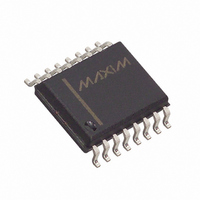
MAX807MEWE+ Maxim Integrated Products, MAX807MEWE+ Datasheet - Page 10

MAX807MEWE+
Manufacturer Part Number
MAX807MEWE+
Description
IC SUPERVISOR MPU 16-SOIC
Manufacturer
Maxim Integrated Products
Type
Battery Backup Circuitr
Datasheet
1.MAX807NEWE.pdf
(16 pages)
Specifications of MAX807MEWE+
Number Of Voltages Monitored
1
Reset
Active High/Active Low
Reset Timeout
140 ms Minimum
Voltage - Threshold
4.575V
Operating Temperature
-40°C ~ 85°C
Mounting Type
Surface Mount
Package / Case
16-SOIC (0.300", 7.5mm Width)
Monitored Voltage
4.425 V
Output Type
Active High, Active Low
Manual Reset
Resettable
Watchdog
Watchdog
Battery Backup Switching
Backup
Supply Voltage (max)
5.5 V
Supply Voltage (min)
0 V
Supply Current (typ)
70 uA
Maximum Power Dissipation
762 mW
Maximum Operating Temperature
+ 85 C
Mounting Style
SMD/SMT
Minimum Operating Temperature
- 40 C
Power Fail Detection
Yes
Undervoltage Threshold
4.35 V
Overvoltage Threshold
4.5 V
Power-up Reset Delay (typ)
280 ms
Lead Free Status / RoHS Status
Lead free / RoHS Compliant
Output
-
Lead Free Status / Rohs Status
Lead free / RoHS Compliant
WDO remains high if there is a transition or pulse at
WDI during the watchdog-timeout period. WDO goes
low if no transition occurs at WDI during the watchdog-
timeout period. The watchdog function is disabled and
WDO is a logic high when V
threshold or WDI is an open circuit. To generate a sys-
tem reset on every watchdog fault, diode-OR connect
WDO to MR (Figure 6). When a watchdog fault occurs
in this mode, WDO goes low, which pulls MR low, caus-
ing a reset pulse to be issued. As soon as reset is
asserted, the watchdog timer clears and WDO returns
high. With WDO connected to MR, a continuous high or
low on WDI will cause 200ms reset pulses to be issued
every 1.6s.
Full-Featured µP Supervisory Circuit with
±1.5% Reset Accuracy
Figure 4. Manual-Reset Timing Diagram
Figure 5. Watchdog Timing Relationship
10
WDO CONNECTED TO µP INTERRUPT.
V
RESET
WDO
WDI
CC
______________________________________________________________________________________
CE OUT
RESET
CE IN
MR
0V
V
RST
t
RP
t
WD
CC
is below the reset
Watchdog Output
170ns
1µs MIN
28µs TYP
The MAX807 provides internal gating of chip-enable
(CE) signals to prevent erroneous data from corrupting
the CMOS RAM in the event of a power failure. During
normal operation, the CE gate is enabled and passes
all CE transitions. When reset is asserted, this path
becomes disabled, preventing erroneous data from
corrupting the CMOS RAM. The MAX807 uses a series
transmission gate from the Chip-Enable Input (CE IN) to
the Chip-Enable Output (CE OUT) (Figure 1).
The 8ns (max) chip-enable propagation from CE IN to
CE OUT enables the MAX807 to be used with most µPs.
CE IN is high impedance (disabled mode) while RESET
is asserted. During a power-down sequence when V
passes the reset threshold, the CE transmission gate
disables and CE IN becomes high impedance 28µs
after reset is asserted (Figure 7). During a power-up
sequence, CE IN remains high impedance (regardless
of
reset-timeout period.
In the high-impedance mode, the leakage currents into
this input are ±1µA (max) over temperature. In the low-
impedance mode, the impedance of CE IN appears as
a 75Ω resistor in series with the load at CE OUT.
The propagation delay through the CE transmission
gate depends on both the source impedance of the
drive to CE IN and the capacitive loading on CE OUT
Figure 6. Generating a Reset on Each Watchdog Fault
V
RESET
WDI
WDO
CE IN activity) until reset is deasserted following the
CC
t
RP
WDO
MR
Chip-Enable Signal Gating
t
WD
MAX807
V
CC
RESET
t
∼
RP
50µs
Chip-Enable Input
4.7kΩ
TO µP
CC


