MCP1702-3302E/TO Microchip Technology, MCP1702-3302E/TO Datasheet - Page 11
MCP1702-3302E/TO
Manufacturer Part Number
MCP1702-3302E/TO
Description
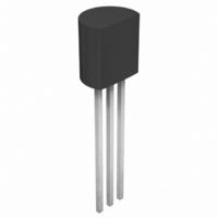
IC REG LDO 3.3V 250MA TO-92-3
Manufacturer
Microchip Technology
Datasheets
1.SOT89-3EV-VREG.pdf
(26 pages)
2.MCP1702T-5002ECB.pdf
(26 pages)
3.MCP1702-3002ETO.pdf
(4 pages)
Specifications of MCP1702-3302E/TO
Package / Case
TO-92-3 (Standard Body), TO-226
Regulator Topology
Positive Fixed
Voltage - Output
3.3V
Voltage - Input
Up to 13.2V
Voltage - Dropout (typical)
0.525V @ 250mA
Number Of Regulators
1
Current - Output
250mA (Min)
Operating Temperature
-40°C ~ 125°C
Mounting Type
Through Hole
Number Of Outputs
1
Polarity
Positive
Input Voltage Max
13.2 V
Output Voltage
3.3 V
Output Type
Fixed
Dropout Voltage (max)
0.725 V at 250 mA
Output Current
250 mA
Line Regulation
0.1 % / V
Load Regulation
1 %
Voltage Regulation Accuracy
0.4 %
Maximum Operating Temperature
+ 125 C
Mounting Style
Through Hole
Minimum Operating Temperature
- 40 C
Primary Input Voltage
4.03V
Output Voltage Fixed
3.3V
Dropout Voltage Vdo
625mV
No. Of Pins
3
Voltage Regulator Case Style
TO-92
Operating Temperature Range
-40°C To +125°C
Rohs Compliant
Yes
Lead Free Status / RoHS Status
Lead free / RoHS Compliant
For Use With
GPIODM-KPLCD - BOARD DEMO LCD GPIO EXP KEYPAD
Current - Limit (min)
-
Lead Free Status / Rohs Status
Lead free / RoHS Compliant
Available stocks
Company
Part Number
Manufacturer
Quantity
Price
Company:

Part Number:
MCP1702-3302E/TO
Manufacturer:
NICHICON
Quantity:
30 000
Part Number:
MCP1702-3302E/TO
Manufacturer:
MICROCHIP/微芯
Quantity:
20 000


3.0
The descriptions of the pins are listed in
TABLE 3-1:
3.1
Regulator ground. Tie GND to the negative side of the
output and the negative side of the input capacitor.
Only the LDO bias current (2.0 µA typical) flows out of
this pin; there is no high current. The LDO output
regulation is referenced to this pin. Minimize voltage
drops between this pin and the negative side of the
load.
3.2
Connect V
positive terminal of the output capacitor. The positive
side of the output capacitor should be physically
located as close to the LDO V
The current flowing out of this pin is equal to the DC
load current.
2010 Microchip Technology Inc.
SOT-23A
Pin No.
1
2
3
–
PIN DESCRIPTIONS
Ground Terminal (GND)
Regulated Output Voltage (V
OUT
to the positive side of the load and the
Pin No.
SOT-89
2, Tab
PIN FUNCTION TABLE
1
3
–
Pin No.
OUT
TO-92
1
3
2
–
pin as is practical.
Table
Symbol
OUT
3-1.
V
GND
V
NC
OUT
IN
)
Ground Terminal
Regulated Voltage Output
Unregulated Supply Voltage
No connection
3.3
Connect V
Like all LDO linear regulators, low source impedance is
necessary for the stable operation of the LDO. The
amount of capacitance required to ensure low source
impedance will depend on the proximity of the input
source
applications, 1 µF of capacitance will ensure stable
operation of the LDO circuit. For applications that have
load currents below 100 mA, the input capacitance
requirement can be lowered. The type of capacitor
used can
electrolytic. The low ESR characteristics of the ceramic
will yield better noise and PSRR performance at
high-frequency.
Unregulated Input Voltage Pin
(V
capacitors
IN
IN
be ceramic, tantalum
to the input unregulated source voltage.
)
Function
or
battery
MCP1702
type.
DS22008E-page 11
or
For
aluminum
most
Related parts for MCP1702-3302E/TO
Image
Part Number
Description
Manufacturer
Datasheet
Request
R

Part Number:
Description:
IC REG LDO 3V 250MA TO-92-3
Manufacturer:
Microchip Technology
Datasheet:
Part Number:
Description:
IC REG LDO 250MA 2.5V TO-92-3
Manufacturer:
Microchip Technology
Datasheet:
Part Number:
Description:
IC REG LDO 1.2V 200MA TO92-3
Manufacturer:
Microchip Technology
Datasheet:
Part Number:
Description:
IC REG LDO 1.8V 200MA TO-92-3
Manufacturer:
Microchip Technology
Datasheet:
Part Number:
Description:
IC REG LDO5V 250MA TO-92-3
Manufacturer:
Microchip Technology
Datasheet:
Part Number:
Description:
Low Iq 250mA LDO, Vin 13.2V Max, Vout=1.5V 3 TO-92 BAG
Manufacturer:
Microchip Technology
Datasheet:
Part Number:
Description:
Low Iq 250mA LDO, Vin 13.2V Max, Vout=4.0V 3 TO-92 BAG
Manufacturer:
Microchip Technology
Datasheet:
Part Number:
Description:
LOW IQ 250MA LDO, VIN 13.2V MAX, VOUT=2.8V
Manufacturer:
Microchip Technology
Datasheet:

Part Number:
Description:
Low Iq 250mA LDO, Vin 13.2V Max, Vout=3.6V 3 TO-92 BAG
Manufacturer:
Microchip Technology
Datasheet:

Part Number:
Description:
HV Low lq LDO, -40C to +125C, 8-SOIC 150mil, TUBE
Manufacturer:
Microchip Technology
Datasheet:
Part Number:
Description:
250 mA Low Quiescent Current LDO Regulator
Manufacturer:
Microchip Technology
Datasheet:

Part Number:
Description:
250 mA Low Quiescent Current LDO Regulator
Manufacturer:
MICROCHIP [Microchip Technology]
Datasheet:
Part Number:
Description:
250 mA Low Quiescent Current LDO Regulator
Manufacturer:
MICROCHIP [Microchip Technology]
Datasheet:
