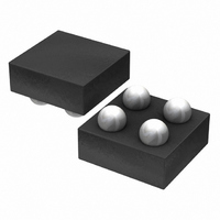
BH30RB1WGUT-E2 Rohm Semiconductor, BH30RB1WGUT-E2 Datasheet - Page 5

BH30RB1WGUT-E2
Manufacturer Part Number
BH30RB1WGUT-E2
Description
IC REG LDO 3.0V 150MA 4-VCSP
Manufacturer
Rohm Semiconductor
Specifications of BH30RB1WGUT-E2
Regulator Topology
Positive Fixed
Voltage - Output
3V
Voltage - Input
Up to 5.5V
Voltage - Dropout (typical)
0.1V @ 100mA
Number Of Regulators
1
Current - Output
150mA (Max)
Operating Temperature
-40°C ~ 85°C
Mounting Type
Surface Mount
Package / Case
4-VCSP
Primary Input Voltage
4V
Output Voltage
3V
Dropout Voltage Vdo
25mV
No. Of Pins
4
Output Current
150mA
Voltage Regulator Case Style
VCSP
Operating Temperature Range
-40°C To +85°C
Svhc
No
Number Of Outputs
1
Polarity
Positive
Input Voltage Max
5.5 V
Output Type
Fixed
Dropout Voltage (max)
150 mV
Line Regulation
20 mV
Load Regulation
2 mV
Voltage Regulation Accuracy
1 %
Maximum Power Dissipation
0.53 W
Maximum Operating Temperature
+ 85 C
Mounting Style
SMD/SMT
Minimum Operating Temperature
- 40 C
Output Voltage Fixed
3V
Rohs Compliant
Yes
Lead Free Status / RoHS Status
Lead free / RoHS Compliant
Current - Limit (min)
-
Lead Free Status / Rohs Status
Lead free / RoHS Compliant
Other names
BH30RB1WGUT-E2TR
Available stocks
Company
Part Number
Manufacturer
Quantity
Price
Company:
Part Number:
BH30RB1WGUT-E2
Manufacturer:
ROHM
Quantity:
3 000
●Block Diagram, Recommended Circuit Diagram, and Pin Assignment Diagram
●Power Dissipation (Pd)
●Input Output Capacitors
© 2011 ROHM Co., Ltd. All rights reserved.
BH□□RB1WGUT series
Fig. 26 Capacitance vs Bias (Y5V)
www.rohm.com
120
100
80
60
40
20
0
VSTBY
1.
2.
It is recommended to insert bypass capacitors between input and GND pins, positioning them as close to the pins as
possible. These capacitors are used when the power supply impedance increases or when long wiring paths are used, so
they should be checked once the IC has been mounted. Ceramic capacitors generally have temperature and DC bias
characteristics. Use X5R or X7R ceramic capacitors, which offer good temperature and DC bias characteristics as well as
stable high voltages.
0
Typical ceramic capacitor characteristics
VIN
10 V torelance
Cin
Power dissipation (Pd)
Power dissipation calculations include output power dissipation characteristics and internal IC power consumption. In
the event that the IC is used in an environment where this power dissipation is exceeded, the attendant rise in the
junction temperature will trigger the thermal shutdown circuit, reducing the current capacity and otherwise degrading the
IC's design performance. Allow for sufficient margins so that this power dissipation is not exceeded during IC operation.
Power dissipation/power dissipation reduction (Pd)
BH□□RB1WGUT
G ND
STBY
1
Calculating the maximum internal IC power consumption (P
VIN
DC bias Vdc (V)
B2
A1
A2
P
2
MAX
16 V torelance
R EF ERE NCE
VO LTAG E
= (V
O VER CU RRE NT
Fig. 25 VCSP60N1 Power Dissipation/Power Dissipation Reduction (Example)
50 V
torelance
P RO T ECT IO N
P RO TE CTIO N
3
TH ERM A L
C O NT RO L
BLO CK
Cin: 1.0 µF
Co: 1.0 µF
IN
Fig. 24
- V
*Circuit design should allow a sufficient margin for the temperature range for PMAX < Pd.
4
OUT
) I
OUT
(MAX.)
100
95
90
85
80
75
70
0.6
0.4
0.2
0
0
VCSP60N1
Fig.27 Capacitance vs Bias
0
B 1
VOUT
25
1
(X5R, X7R)
10 V torelance
DC bias Vdc (V)
VOUT
Co
50
Ta[ ℃ ]
2
530 mW
16 V torelance
5/8
50 V torelance
75
3
MAX
100
V
V
I
Pin No.
OUT
IN
OUT
)
B2
B1
A1
A2
: Input voltage
125
4
(MAX): Output current
: Output voltage
Board: 7 mm 7 mm 0.8 mm
Material: Glass epoxy PCB
Symbol
STBY
1PIN MARK
V
GND
V
OUT
IN
Fig. 28 Capacitance vs Temperature
120
100
80
60
40
20
0
-25
TOP VIEW (Mark side)
A
B
Power supply input
Voltage output
Ground
Output voltage on/off control
(High: ON, Low: OFF)
(X5R, X7R, Y5V)
1
0
Y5V
Temp[ ℃ ]
2
Function
Technical Note
25
2011.01 - Rev.C
X7R
X5R
50
75


