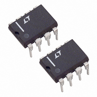
LT1175IN8 Linear Technology, LT1175IN8 Datasheet - Page 10

LT1175IN8
Manufacturer Part Number
LT1175IN8
Description
IC LDO REG ADJST NEG 500MA 8-DIP
Manufacturer
Linear Technology
Datasheet
1.LT1175CN8-5PBF.pdf
(20 pages)
Specifications of LT1175IN8
Regulator Topology
Negative Adjustable
Voltage - Output
-3.8 ~ -19.9 V
Voltage - Input
-4.3 ~ -20 V
Voltage - Dropout (typical)
0.5V @ 500mA
Number Of Regulators
1
Current - Output
500mA
Current - Limit (min)
Adjustable
Operating Temperature
-40°C ~ 85°C
Mounting Type
Through Hole
Package / Case
8-DIP (0.300", 7.62mm)
Lead Free Status / RoHS Status
Contains lead / RoHS non-compliant
Available stocks
Company
Part Number
Manufacturer
Quantity
Price
Company:
Part Number:
LT1175IN8-5
Manufacturer:
LT
Quantity:
14
LT1175
APPLICATIONS INFORMATION
normally a good thing when the regulator is used by itself,
but it prevents the user from shutting down the regulator
when a second power source is connected to the LT1175
output. If active output pull-down is needed in shutdown,
it can be added externally with a depletion mode PFET as
shown in Figure 2. Note that the maximum pinch-off volt-
age of the PFET must be less than the positive logic high
level to ensure that the device is completely off when the
regulator is active. The Motorola J177 device has 300Ω
on resistance for zero gate source voltage.
Minimum Dropout Voltage
Dropout voltage is the minimum voltage required between
input and output to maintain proper output regulation.
For older 3-terminal regulator designs, dropout voltage
was typically 1.5V to 3V. The LT1175 uses a saturating
power transistor design which gives much lower dropout
voltage, typically 100mV at light loads and 450mV at full
load. Special precautions were taken to ensure that this
technique does not cause quiescent supply current to be
high under light load conditions. When the regulator input
voltage is too low to maintain a regulated output, the pass
transistor is driven hard by the error amplifi er as it tries
to maintain regulation. The current drawn by the driver
transistor could be tens of milliamperes even with little or
no load on the output. This indeed was the case for older
IC designs that did not actively limit driver current when
the power transistor saturated. The LT1175 uses a new
antisaturation technique that prevents high driver current,
10
–V
Figure 2. Active Output Pull-Down During Shutdown
IN
+
* MOTOROLA J177
PINCH-OFF VOLTAGE MUST BE LESS THAN
POSITIVE LOGIC HIGH VOLTAGE
3V TO 5V
V
I
I
LIM2
LIM4
IN
SHDN
LT1175-5
GND
OUTPUT
SENSE
Q1*
s
d
C
≥ 0.1μF
1175 F02
OUT
yet allows the power transistor to approach its theoretical
saturation limit.
Output Capacitor
Several new regulator design techniques are used to make
the LT1175 extremely tolerant of output capacitor selection.
Like most low dropout designs which use a collector or
drain of the power transistor to drive the output node, the
LT1175 uses the output capacitor as part of the overall
loop compensation. Older regulators generally required
the output capacitor to have a minimum value of 1μF to
100μF , a maximum ESR (Effective Series Resistance) of
0.1Ω to 1Ω and a minimum ESR in the range of 0.03Ω to
0.3Ω. These restrictions usually could be met only with
good quality solid tantalum capacitors. Aluminum capaci-
tors have problems with high ESR unless much higher
values of capacitance are used (physically large). The ESR
of ceramic or fi lm capacitors was too low, which made
the capacitance/ESR zero frequency too high to maintain
phase margin in the regulator. Even with optimum capaci-
tors, loop phase margin was very low in previous designs
when output current was low. These problems led to a new
design technique for the LT1175 error amplifi er and internal
frequency compensation as shown in Figure 3.
A conventional regulator loop consists of error amplifi er
A1, driver transistor Q2 and power transistor Q1. Added
to this basic loop are secondary loops generated by Q3
and C
amplifi er through Q3 and R
gain to be very low at light load currents. This is not a
problem because very little gain is needed at light loads.
In addition to low gain, the parasitic pole frequency at Q2
base is extended by the DC feedback. The combination of
these two effects dramatically improves loop phase margin
at light loads and makes the loop tolerant of large ESR in
the output capacitor. With heavy loads, loop phase and gain
are not nearly as troublesome and large negative feedback
could degrade regulation. The logarithmic behavior of the
base emitter voltage of Q1 reduces Q3 negative feedback
at heavy loads to prevent poor regulation.
In a conventional design, even with the nonlinear feedback,
poor loop phase margin would occur at medium to heavy
loads if the ESR of the output capacitor fell below 0.3Ω.
F
. A DC negative feedback current fed into the error
N
causes overall loop current
1175ff


