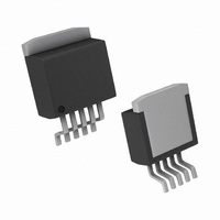
LP3872ESX-3.3/NOPB National Semiconductor, LP3872ESX-3.3/NOPB Datasheet - Page 14

LP3872ESX-3.3/NOPB
Manufacturer Part Number
LP3872ESX-3.3/NOPB
Description
IC REG LDO 1.5A 3.3V TO-263-5
Manufacturer
National Semiconductor
Datasheet
1.LP3872EMP-3.3NOPB.pdf
(18 pages)
Specifications of LP3872ESX-3.3/NOPB
Regulator Topology
Positive Fixed
Voltage - Output
3.3V
Voltage - Input
Up to 7V
Voltage - Dropout (typical)
0.38V @ 1.5A
Number Of Regulators
1
Current - Output
1.5A (Max)
Operating Temperature
-40°C ~ 125°C
Mounting Type
Surface Mount
Package / Case
TO-263-5, D²Pak (5 leads + Tab), TO-263BA
Lead Free Status / RoHS Status
Lead free / RoHS Compliant
Current - Limit (min)
-
Other names
LP3872ESX-3.3
Available stocks
Company
Part Number
Manufacturer
Quantity
Price
Company:
Part Number:
LP3872ESX-3.3/NOPB
Manufacturer:
TI
Quantity:
12 000
www.national.com
Application Hints
DROPOUT VOLTAGE
The dropout voltage of a regulator is defined as the minimum
input-to-output differential required to stay within 2% of the
nominal output voltage. For CMOS LDOs, the dropout volt-
age is the product of the load current and the Rds(on) of the
internal MOSFET.
REVERSE CURRENT PATH
The internal MOSFET in LP3872 and LP3875 has an inher-
ent parasitic diode. During normal operation, the input volt-
age is higher than the output voltage and the parasitic diode
is reverse biased. However, if the output is pulled above the
input in an application, then current flows from the output to
the input as the parasitic diode gets forward biased. The
output can be pulled above the input as long as the current
in the parasitic diode is limited to 200mA continuous and 1A
peak.
POWER DISSIPATION/HEATSINKING
LP3872 and LP3875 can deliver a continuous current of
1.5A over the full operating temperature range. A heatsink
may be required depending on the maximum power dissipa-
tion and maximum ambient temperature of the application.
Under all possible conditions, the junction temperature must
be within the range specified under operating conditions.
The total power dissipation of the device is given by:
P
where I
(specified under Electrical Characteristics).
The maximum allowable temperature rise (T
on the maximum ambient temperature (T
cation, and the maximum allowable junction temperature
(T
T
The maximum allowable value for junction to ambient Ther-
mal Resistance, θ
θ
LP3872 and LP3875 are available in TO-220 and TO-263
packages. The thermal resistance depends on amount of
copper area or heat sink, and on air flow. If the maximum
allowable value of θ
TO-220 package and ≥ 60 ˚C/W for TO-263 package no
heatsink is needed since the package can dissipate enough
heat to satisfy these requirements. If the value for allowable
θ
HEATSINKING TO-220 PACKAGE
The thermal resistance of a TO220 package can be reduced
by attaching it to a heat sink or a copper plane on a PC
board. If a copper plane is to be used, the values of θ
be same as shown in next section for TO263 package.
The heatsink to be used in the application should have a
heatsink to ambient thermal resistance,
θ
In this equation, θ
to the surface of the heat sink and θ
tance from the junction to the surface of the case. θ
about 3˚C/W for a TO220 package. The value for θ
pends on method of attachment, insulator, etc. θ
between 1.5˚C/W to 2.5˚C/W. If the exact value is unknown,
2˚C/W can be assumed.
JA
JA
HA
Rmax
D
Jmax
= (V
≤ θ
= T
falls below these limits, a heat sink is required.
):
= T
JA
Rmax
GND
IN
−V
− θ
Jmax
OUT
/ P
is the operating ground current of the device
CH
− T
D
)I
− θ
OUT
Amax
CH
JA
JC
, can be calculated using the formula:
JA
is the thermal resistance from the case
+ (V
.
calculated above is ≥ 60 ˚C/W for
IN
)I
GND
(Continued)
JC
is the thermal resis-
Amax
Rmax
) of the appli-
) depends
CH
CH
varies
JA
JC
de-
will
is
14
HEATSINKING TO-263 PACKAGE
The TO-263 package uses the copper plane on the PCB as
a heatsink. The tab of these packages are soldered to the
copper plane for heat sinking. Figure 3 shows a curve for the
θ
a typical PCB with 1 ounce copper and no solder mask over
the copper area for heat sinking.
As shown in the figure, increasing the copper area beyond 1
square inch produces very little improvement. The minimum
value for θ
32˚C/W.
Figure 4 shows the maximum allowable power dissipation
for TO-263 packages for different ambient temperatures,
assuming θ
ture is 125˚C.
HEATSINKING SOT223-5 PACKAGE
Figure 5 shows a curve for the θ
different copper area sizes, using a typical PCB with 1 ounce
copper and no solder mask over the copper area for heat
sinking.
JA
FIGURE 3. θ
FIGURE 4. Maximum power dissipation vs ambient
of TO-263 package for different copper area sizes, using
JA
JA
temperature for TO-263 package
for the TO-263 package mounted to a PCB is
is 35˚C/W and the maximum junction tempera-
JA
vs Copper (1 Ounce) Area for TO-263
package
JA
of SOT-223 package for
20063332
20063333


