LP2960AIM-3.3/NOPB National Semiconductor, LP2960AIM-3.3/NOPB Datasheet - Page 11
LP2960AIM-3.3/NOPB
Manufacturer Part Number
LP2960AIM-3.3/NOPB
Description
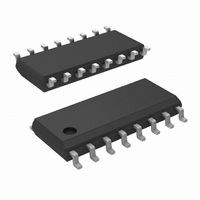
IC REG LDO 3.3V 500MA 16-SOIC
Manufacturer
National Semiconductor
Datasheet
1.LP2960IM-5.0NOPB.pdf
(16 pages)
Specifications of LP2960AIM-3.3/NOPB
Regulator Topology
Positive Fixed
Voltage - Output
3.3V
Voltage - Input
Up to 30V
Voltage - Dropout (typical)
0.47V @ 500mA
Number Of Regulators
1
Current - Output
500mA
Operating Temperature
-40°C ~ 125°C
Mounting Type
Surface Mount
Package / Case
16-SOIC (3.9mm Width)
Lead Free Status / RoHS Status
Lead free / RoHS Compliant
Current - Limit (min)
-
Other names
*LP2960AIM-3.3
*LP2960AIM-3.3/NOPB
LP2960AIM-3.3
*LP2960AIM-3.3/NOPB
LP2960AIM-3.3
Available stocks
Company
Part Number
Manufacturer
Quantity
Price
Company:

Part Number:
LP2960AIM-3.3/NOPB
Manufacturer:
NS
Quantity:
140


Application Hints
EXTERNAL CAPACITORS
Bypass capacitors on the input and output of the LP2960 are
required: without these capacitors, the part will oscillate.
A capacitor (whose value is at least 4.7 µF) must be con-
nected from the V
located more than one inch away from the LP2960, the
capacitor may have to be increased to 22 µF to assure
stability. A capacitor is also required between V
Ground, and the minimum amount of capacitance required
here depends on output voltage.
If the output voltage of the LP2960 is set to 5V, a minimum of
10 µF is needed in output capacitance. At 3.3V output, at
least 22 µF is required to assure stability.
ESR LIMIT: The ESR of the capacitor used on the LP2960
must be less than 0.7Ω throughout the entire operating
temperature range to assure stability.
The ESR of an aluminum eIectroIytic capacitor is typically
only specified at 25˚C, and does not reflect the maximum
ESR that can be expected to occur over the entire tempera-
ture range of the capacitor.
Aluminum electrolytics show a marked increase in ESR at
low temperatures (ESR can increase by a factor of 30 or
more when going from 25˚C to −30˚C) which could lead to
oscillation probIems in applications with very low ambient
temperatures. Solid tantalum capacitors are recommended
for use in such cases.
Regulator instability can be caused by stray (board layout)
capacitance appearing at the Feedback terminal. Oscilla-
tions from this effect are most Iikely to occur when very high
value resistors are used to set the output voltage.
Adding a 100 pF capacitor between the Output and Feed-
back pins and increasing the output capacitor to at least
22 µF will stop the osciIIations.
MINIMUM LOAD
The internal resistive divider in the LP2960 provides suffi-
cient output loading for proper regulation. If externaI resis-
tors are used to set the LP2960 output voltage, a minimum
current of 5 µA through the externaI resistive divider is
recommended.
It should be noted that a minimum load current is specified in
several of the test conditions listed under Electrical Charac-
teristics, and this value of load current must be used to get
correlation on these test limits.
PROGRAMMING THE OUTPUT VOLTAGE
The LP2960 regulator may be pin-strapped for operation at
the nominal output voltage using its internal resistive divider
by tying the Output and Sense pins together and also tying
the Feedback and V
Alternatively, it may be programmed for any voltage between
the 1.23V reference and the 30V maximum rating using an
external pair of resistors (see Basic Application Circuit).
The complete equation for the output voltage is:
The term V
back pin bias current (−20 nA typical). The minimum recom-
mended load current of 5 µA sets an upper limit of 240 kΩ on
the value of R2 in cases where the regulator must work with
no load (see Minimum Load).
V
OUT
REF
= V
is the 1 .23V reference and I
IN
REF
TAP
pin to ground. If the input capacitor is
x (1 + R1/R2) + (I
pins together.
FB
x R1)
FB
is the Feed-
OUT
and
11
For best output accuracy, choosing R2 = 100 kΩ will reduce
the error resulting from I
resistive divider current to 12 µA. Since the typicaI quiescent
current of the LP2960 is 450 µA, this added current through
R2 is negligible.
DROPOUT VOLTAGE
The dropout voltage of the regulator is defined as the mini-
mum input-to-output voltage differential required for the out-
put voltage to stay within 100 mV of the output voltage
measured with a 1V differential. The dropout voltage is in-
dependent of the programmed output voltage.
OUTPUT ISOLATION
If the LP2960 output is connected to an active voltage
source (such as a battery) the regulator input should not be
shorted to ground, as this will cause a large current to flow
from the battery into the LP2960 output lead.
If the LP2960 input is left floating with the output connected
to a battery, a small current (a few mA) will flow into the
output lead.
The “reverse” current flowing from the battery into the
LP2960 output can be prevented by using a blocking diode
between the output and the battery.
REDUCING OUTPUT NOISE
In reference applications it may be desirabIe to reduce the
AC noise present on the output. One method is to reduce
regulator bandwidth by increasing output capacitance. This
is relatively inefficient, since large increases in capacitance
are required to get significant improvement.
Noise can be reduced more effectively by a bypass capacitor
placed across R1 (refer to Basic Application Circuit).
A 0.1 µF capacitor connected across R1 will reduce the high
frequency gain of the circuit to unity, lowering the RMS
output noise voltage from 210 µV to 130 µV (typical) using a
10 Hz–100 kHz bandwidth test measurement.
Also, output noise is no longer proportional to the output
voltage, so improvements are more pronounced at higher
output voltages.
IMPORTANT: Since the 0.1 µF capacitor reduces the AC
gain of the LP2960 to unity, the output capacitance must be
increased to at least 33 µF to assure regulator stability.
DROPOUT DETECTION COMPARATOR
The dropout detection comparator produces a logic “LOW”
on the Error output whenever the LP2960 output drops out of
regulation by more than about 5%. This figure results from
the comparator’s built-in offset of 60 mV divided by the 1.23V
reference (refer to block diagram).
The “5% below nominal” trip level remains constant regard-
less of the programmed output voltage. An out-of-regulation
condition can result from low input voltage, current limiting,
or thermal limiting.
The figure below gives a timing diagram showing the rela-
tionship between the output voltage, the Error output, and
input voltage as the input voltage is ramped up and down to
a regulator programmed for 5V output.
FB
to 0.17% while increasing the
www.national.com
Related parts for LP2960AIM-3.3/NOPB
Image
Part Number
Description
Manufacturer
Datasheet
Request
R

Part Number:
Description:
Manufacturer:
National Semiconductor
Datasheet:
Part Number:
Description:
IC REG LDO 5V 500MA 16-SOIC
Manufacturer:
National Semiconductor
Datasheet:

Part Number:
Description:
IC REG LDO 5V 500MA 16-SOIC
Manufacturer:
National Semiconductor
Datasheet:
Part Number:
Description:
National Semiconductor [8-Bit D/A Converter]
Manufacturer:
National Semiconductor
Datasheet:
Part Number:
Description:
National Semiconductor [Media Coprocessor]
Manufacturer:
National Semiconductor
Datasheet:
Part Number:
Description:
Digitally Controlled Tone and Volume Circuit with Stereo Audio Power Amplifier, Microphone Preamp Stage and National 3D Sound
Manufacturer:
National Semiconductor
Datasheet:
Part Number:
Description:
Digitally Controlled Tone and Volume Circuit with Stereo Audio Power Amplifier, Microphone Preamp Stage and National 3D Sound
Manufacturer:
National Semiconductor
Datasheet:
Part Number:
Description:
AC97 Rev 2 Codec with Sample Rate Conversion and National 3D Sound
Manufacturer:
National Semiconductor
Part Number:
Description:
Manufacturer:
National Semiconductor
Datasheet:
Part Number:
Description:
Manufacturer:
National Semiconductor
Datasheet:
Part Number:
Description:
General Purpose, Low Voltage, Low Power, Rail-to-Rail Output Operational Amplifiers
Manufacturer:
National Semiconductor
Datasheet:
Part Number:
Description:
8-bit 20 MSPS flash A/D converter.
Manufacturer:
National Semiconductor
Datasheet:
Part Number:
Description:
Low Noise Quad Operational Amplifier
Manufacturer:
National Semiconductor
Datasheet:
Part Number:
Description:
Quad Differential Line Receivers
Manufacturer:
National Semiconductor
Datasheet: