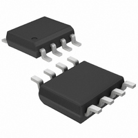
MAX667ESA+T Maxim Integrated Products, MAX667ESA+T Datasheet - Page 3

MAX667ESA+T
Manufacturer Part Number
MAX667ESA+T
Description
IC REG LDO 5V/ADJ 8-SOIC
Manufacturer
Maxim Integrated Products
Type
Linearr
Datasheet
1.MAX667CPA.pdf
(9 pages)
Specifications of MAX667ESA+T
Regulator Topology
Positive Fixed or Adjustable
Voltage - Output
5V, 1.3 ~ 16 V
Voltage - Input
3.5 ~ 16.5 V
Voltage - Dropout (typical)
0.15V @ 250mA
Number Of Regulators
1
Current - Output
250mA (Min)
Operating Temperature
-40°C ~ 85°C
Mounting Type
Surface Mount
Package / Case
8-SOIC (3.9mm Width)
Package
8SOIC N
Function
LDO
Number Of Outputs
1
Input Voltage Range
16.5 to 3.5 V
Output Voltage
1.3 to 16|5 V
Maximum Output Current
0.25(Min) A
Output Type
Adjustable|Fixed
Typical Dropout Voltage @ Current
0.005@100uA|0.15@200mA V
Polarity
Positive
Reference Voltage
1.225(Typ) V
Input Voltage Max
16.5 V
Dropout Voltage (max)
0.06 V at 100 uA
Output Current
250 mA
Line Regulation
10 mV
Load Regulation
100 mV
Maximum Power Dissipation
0.471 W
Maximum Operating Temperature
+ 85 C
Mounting Style
SMD/SMT
Minimum Operating Temperature
- 40 C
Lead Free Status / RoHS Status
Lead free / RoHS Compliant
Current - Limit (min)
-
Lead Free Status / Rohs Status
Lead free / RoHS Compliant
_____________________Pin Description
(T
__________________________________________Typical Operating Characteristics
A
PIN
1000
= +25°C, unless otherwise noted.)
100
1
2
3
4
5
6
7
8
10
1
1
NAME
SHDN
GND
OUT
LBO
SET
DD
LBI
IN
DROPOUT VOLTAGE
vs. LOAD CURRENT
LOAD CURRENT (mA)
10
_______________________________________________________________________________________
Dropout Detector Output—the collec-
tor of a PNP pass transistor. Normally
an open circuit, it sources current as
dropout is reached.
Regulated Output Voltage. OUT falls
to 0V when SHDN is above 1.5V. SET
determines output voltage when SET
is above 50mV; otherwise, it is 5V.
OUT must be connected to an output
filter capacitor.
Low-Battery Detector. A CMOS input
to an internal 1.255V comparator
whose output is the LBO pin.
Ground
Shutdown Input. Connect to GND for
normal operation (output active). Pull
above 1.5V to disable OUT, LBO, and
DD and to reduce quiescent current to
less than 1µA.
(Output) Voltage Set, CMOS Input.
Connect to GND for 5V output. For
other voltages, connect external resis-
tive divider from OUT.
Low-Battery Output. An open-drain N-
channel transistor that sinks current to
GND when LBI is less than 1.22V.
Positive Input Voltage (unregulated)
100
FUNCTION
1000
+5V/Programmable Low-Dropout
100,000
10,000
1000
100
10
0.01
V IN = +6V
0.1
QUIESCENT CURRENT
vs. LOAD CURRENT
LOAD CURRENT (mA)
1
Figure 1 shows a micropower bandgap reference, an
error amplifier, a PNP pass transistor, and two com-
parators as the main elements of the MAX667. One
comparator, C1, selects the fixed 5V or adjustable
operation with an external voltage divider. The other
comparator, C2, is a low-battery detector.
The bandgap reference, which is trimmed to 1.22V,
connects internally to one input of the error amplifier,
A1. The feedback signal from the regulator output sup-
plies the other input of A1 from either an on-chip volt-
age divider or two external resistors. When SET is
grounded, the internal divider provides the error ampli-
fier feedback signal for a fixed 5V output. When SET is
more than 50mV above ground, the error amplifier’s
input switches directly to SET while an external resistor
divider from OUT determines the output voltage.
A second comparator, C2, compares the LBI input to
the internal reference voltage. LBO is an open-drain
FET connected to GND. The low-battery threshold can
also be set with a voltage divider at LBI. In addition, the
MAX667 has a shutdown input (SHDN) that disables
the load and the device while reducing quiescent cur-
rent when it is pulled high.
Figure 2 shows the connection for a fixed 5V output.
The SET input is grounded, and no external resistors
are required. Figure 3 shows adjustable output opera-
tion. R1 and R2 set the output voltage. SHDN should be
grounded if not used.
_______________Detailed Description
10
100
Voltage Regulator
1000
1000
100
10
1
0
5 10
1
vs. INPUT-OUTPUT DIFFERENCE
2
INPUT-OUTPUT DIFFERENCE (mV)
50
DD OUTPUT CURRENT
20 50 100mA LOAD
100
150
+5V Output
200
250
3


