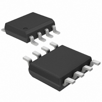
MAX667ESA+T Maxim Integrated Products, MAX667ESA+T Datasheet - Page 5

MAX667ESA+T
Manufacturer Part Number
MAX667ESA+T
Description
IC REG LDO 5V/ADJ 8-SOIC
Manufacturer
Maxim Integrated Products
Type
Linearr
Datasheet
1.MAX667CPA.pdf
(9 pages)
Specifications of MAX667ESA+T
Regulator Topology
Positive Fixed or Adjustable
Voltage - Output
5V, 1.3 ~ 16 V
Voltage - Input
3.5 ~ 16.5 V
Voltage - Dropout (typical)
0.15V @ 250mA
Number Of Regulators
1
Current - Output
250mA (Min)
Operating Temperature
-40°C ~ 85°C
Mounting Type
Surface Mount
Package / Case
8-SOIC (3.9mm Width)
Package
8SOIC N
Function
LDO
Number Of Outputs
1
Input Voltage Range
16.5 to 3.5 V
Output Voltage
1.3 to 16|5 V
Maximum Output Current
0.25(Min) A
Output Type
Adjustable|Fixed
Typical Dropout Voltage @ Current
0.005@100uA|0.15@200mA V
Polarity
Positive
Reference Voltage
1.225(Typ) V
Input Voltage Max
16.5 V
Dropout Voltage (max)
0.06 V at 100 uA
Output Current
250 mA
Line Regulation
10 mV
Load Regulation
100 mV
Maximum Power Dissipation
0.471 W
Maximum Operating Temperature
+ 85 C
Mounting Style
SMD/SMT
Minimum Operating Temperature
- 40 C
Lead Free Status / RoHS Status
Lead free / RoHS Compliant
Current - Limit (min)
-
Lead Free Status / Rohs Status
Lead free / RoHS Compliant
If SET is connected to a resistive voltage divider (Figure
3), the output voltage is set by the equation:
where V
To simplify resistor selection:
Since the input bias current at SET has a maximum
value of 10nA, relatively large values can be used for
R1 and R2 with no loss of accuracy. 1MΩ is a typical
value for R1. The V
This allows the output to be preset without trim pots,
using only fixed resistors in most cases. However, when
resistor values greater than 1MΩ are used, pay special
attention to printed circuit board leakage that can intro-
duce error at the SET input.
SHDN puts the device into standby mode to conserve
power. When this pin is held low, the IC operates nor-
mally. If it is driven above 1.5V, the chip shuts down.
Quiescent current of the MAX667 is then reduced to
less than 1µA, and OUT turns off.
Note that the voltage for SHDN must never be more
than 0.3V higher than V
The MAX667 contains circuitry for low-battery detec-
tion. If the voltage at LBI falls below the regulator’s
internal reference (1.22V), LBO, an open-drain output,
sinks current to GND. The threshold can be set to any
level above the reference voltage by connecting a
resistive divider to LBI based on the equation:
where V
detector, and R3 and R4 are the LBI input divider
resistors.
Since LBI input current is no more than 10nA, high val-
ues for R3 and R4 minimize loading. If V
5.5V low-battery threshold can be set using 8.2MΩ for
R3 and 2.4MΩ for R4. When resistor values greater
than 1MΩ are used, pay special attention to PC board
leakage that can introduce error at the LBI input.
When the voltage at LBI is below the internal threshold,
LBO sinks current to GND. A pull-up resistor of 10kΩ or
more connected to OUT can be used with this pin when
driving CMOS circuits. Any pull-up resistor connected
to LBO should not be returned to a voltage source
greater than V
the MAX667 is in SHDN mode, the LBO output is off.
SET
BATT
V
R2 = R1 x (V
R3 = R4 x (V
OUT
= 1.22V
is the desired threshold of the low-battery
OUT
= V
_______________________________________________________________________________________
. When LBI is above the threshold or
SET
SET
Shutdown (Standby) Mode
OUT
BATT
Output-Voltage Selection
IN
x (R1 + R2) / R1,
tolerance is less than ±25mV.
.
/ V
Low-Battery Function
/ V
SET
LBI
- 1)
- 1)
+5V/Programmable Low-Dropout
OUT
is 5V, a
The minimum input-output differential, or dropout volt-
age, determines the regulator’s lowest usable input
voltage. In battery-operated systems, this determines
the useful end-of-life battery voltage. The MAX667 fea-
tures very low dropout voltage (see Electrical
Characteristics). In addition, the MAX667 has a dropout
detector output, DD, that changes as the dropout volt-
age approaches its limit. DD is an open collector of a
PNP transistor. The dropout voltage and the dropout
detector both depend on the output current and tem-
perature. When the input voltage is more than 300mV
above the output voltage, the dropout detector will not
conduct. As the differential decreases below 300mV,
the DD source current increases abruptly. This current
signals a warning that regulation is about to be lost.
Connecting a resistor (typically 100kΩ) from DD to
ground develops a voltage that can be monitored by
analog circuits or changed to digital levels by a com-
parator. LBI may be used for this purpose.
As with all PNP output regulators, an output capacitor
(C1, Figure 2) is required to maintain stability. 10µF is
recommended. To ensure stability, the output-capacitor
ESR must be sufficiently high. Figure 4 shows the mini-
mum required output-capacitor ESR for a given temper-
ature. Alternatively, a resistor may be added in series
with the output capacitor (Figure 5); the sum of the out-
Figure 4. Minimum Required Output-Capacitor ESR vs.
Temperature
__________Applications Information
5
4
3
2
1
0
Voltage Regulator
-60 -40 -20
TEMPERATURE (˚C)
0
20 40 60 80 100 120
Dropout Detector
Output Capacitor
5


