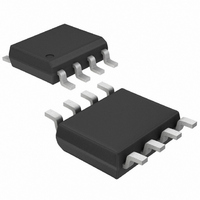
MAX667ESA+T Maxim Integrated Products, MAX667ESA+T Datasheet - Page 8

MAX667ESA+T
Manufacturer Part Number
MAX667ESA+T
Description
IC REG LDO 5V/ADJ 8-SOIC
Manufacturer
Maxim Integrated Products
Type
Linearr
Datasheet
1.MAX667CPA.pdf
(9 pages)
Specifications of MAX667ESA+T
Regulator Topology
Positive Fixed or Adjustable
Voltage - Output
5V, 1.3 ~ 16 V
Voltage - Input
3.5 ~ 16.5 V
Voltage - Dropout (typical)
0.15V @ 250mA
Number Of Regulators
1
Current - Output
250mA (Min)
Operating Temperature
-40°C ~ 85°C
Mounting Type
Surface Mount
Package / Case
8-SOIC (3.9mm Width)
Package
8SOIC N
Function
LDO
Number Of Outputs
1
Input Voltage Range
16.5 to 3.5 V
Output Voltage
1.3 to 16|5 V
Maximum Output Current
0.25(Min) A
Output Type
Adjustable|Fixed
Typical Dropout Voltage @ Current
0.005@100uA|0.15@200mA V
Polarity
Positive
Reference Voltage
1.225(Typ) V
Input Voltage Max
16.5 V
Dropout Voltage (max)
0.06 V at 100 uA
Output Current
250 mA
Line Regulation
10 mV
Load Regulation
100 mV
Maximum Power Dissipation
0.471 W
Maximum Operating Temperature
+ 85 C
Mounting Style
SMD/SMT
Minimum Operating Temperature
- 40 C
Lead Free Status / RoHS Status
Lead free / RoHS Compliant
Current - Limit (min)
-
Lead Free Status / Rohs Status
Lead free / RoHS Compliant
+5V/Programmable Low-Dropout
Voltage Regulator
(PSRR) is therefore not specified. Since the output must
be connected to a 10µF or larger filter capacitor, the
capacitor characteristics dominate the PSRR. Large
values of input and output capacitors reduce the ripple.
In addition, both DD and LBI/LBO can trigger on the
lowest DC component of the ripple, particularly at high
load currents. In the case of the low-battery detector,
the ripple can be effectively filtered out by placing a
capacitor to ground in parallel with the LBI input pin.
The high resistance values that can be used for the
voltage divider allow relatively small capacitance val-
ues to form an effective lowpass filter at 120Hz. When
power is first applied, however, this filter tends to hold
LBO low longer than normal.
The low operating current and gain-bandwidth product
of the internal reference and amplifier result in limited
rejection of fast-step input changes. Negative-going
steps, which occur in under 100µs, may turn off the out-
put for several milliseconds. An input filter (nominally
10µF) is recommended if input changes greater than
1V and faster than 100µs (other than turn-on or turn-off)
are anticipated. Figure 12 shows the output response to
a 10mA/100mA instantaneous load step. The relation-
ship between output-capacitor ESR and load-transient
response is explained in the Output Capacitor section.
Figure 12. Output Response to 10mA/100mA Load Step with
10 μ F Output Capacitor (1.5 Ω ESR)
8
CURRENT
+5V OUTPUT
OUTPUT
_______________________________________________________________________________________
0.1V/div
100mA
10mA
Transient Considerations
200μs/div
TRANSISTOR COUNT: 65
SUBSTRATE MUST BE LEFT UNCONNECTED
For the latest package outline information and land patterns,
go to www.maxim-ic.com/packages.
___________________Chip Topography
PACKAGE TYPE
OUT
LBI
8 CERDIP
8 PDIP
8 SO
GND
DD
PACKAGE CODE
(1.78mm)
0.070"
Package Information
IN
P8-T
S8-4
J8-2
SHDN
DOCUMENT NO.
LBO
SET
(2.71mm)
21-0043
21-0041
21-0045
0.107"


