ADP3331ART-REEL Analog Devices Inc, ADP3331ART-REEL Datasheet
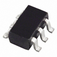
IC REG LDO ADJ 200MA SOT-23-6

ADP3331ART-REEL

Manufacturer Part Number
ADP3331ART-REEL
Description
IC REG LDO ADJ 200MA SOT-23-6
Manufacturer
Analog Devices Inc
Series
anyCAP®r
Datasheet

Specifications of ADP3331ART-REEL

Rohs Status
RoHS non-compliant
Regulator Topology
Positive Adjustable
Voltage - Output
1.5 ~ 11.75 V
Voltage - Input
2.6 ~ 12 V
Voltage - Dropout (typical)
0.14V @ 200mA
Number Of Regulators
1
Current - Output
200mA
Operating Temperature
-40°C ~ 85°C
Mounting Type
Surface Mount
Package / Case
SOT-23-6
Current - Limit (min)
-

Available stocks

Company
Part Number
Manufacturer
Quantity
Price
Part Number:
ADP3331ART-REEL7
Manufacturer:
AD
Quantity:
155 170
a
REV. A
GENERAL DESCRIPTION
The ADP3331 is a member of the ADP330x family of precision
low dropout anyCAP voltage regulators. The ADP3331 operates
with an input voltage range of 2.6 V to 12 V and delivers a load
current up to 200 mA. The ADP3331 stands out from the
conventional LDOs with a novel architecture and an enhanced
process that enables it to offer performance advantages and higher
output current than its competition. Its patented design requires
only a 0.47 mF output capacitor for stability. This device is insensi-
tive to capacitor equivalent series resistance (ESR), and is stable
with any good quality capacitor, including ceramic (MLCC) types
Information furnished by Analog Devices is believed to be accurate and
reliable. However, no responsibility is assumed by Analog Devices for its
use, nor for any infringements of patents or other rights of third parties that
may result from its use. No license is granted by implication or otherwise
under any patent or patent rights of Analog Devices. Trademarks and
registered trademarks are the property of their respective companies.
FEATURES
High Accuracy over Line and Load:
Ultralow Dropout Voltage: 140 mV (Typ) @ 200 mA
Can Be Used as a High Current (>1 A) LDO
Requires Only C
anyCAP = Stable with Any Type of Capacitor
Current and Thermal Limiting
Low Noise
Low Shutdown Current: 10 nA Typical
2.6 V to 12 V Supply Range
1.5 V to 11.75 V Output Range
–40 C to +85 C Ambient Temperature Range
Ultrasmall Thermally Enhanced Chip-on-Lead™
APPLICATIONS
Cellular Telephones
Notebook, Palmtop Computers
Battery-Powered Systems
PCMCIA Regulators
Bar Code Scanners
Camcorders, Cameras
1.4% over Temperature
Controller
(Including MLCC)
SOT-23-6 Lead Package
O
= 0.47 F for Stability
0.7% @ 25 C,
SOT-23, anyCAP
Adjustable Output Ultralow I
for space restricted applications. The ADP3331 achieves excep-
tional accuracy of ± 0.7% at room temperature and ± 1.4% overall
accuracy over temperature, line, and load variations. The drop-
out voltage of the ADP3331 is only 140 mV (typical) at 200 mA.
This device also includes a safety current limit, thermal over-
load protection, and a shutdown feature. In shutdown mode, the
ground current is reduced to less than 2 mA. The ADP3331 has
ultralow quiescent current 34 mA (typical) in light load situations.
The SOT-23-6 package has been thermally enhanced using
Analog Device’s proprietary Chip-on-Lead feature to maxi-
mize power dissipation.
One Technology Way, P.O. Box 9106, Norwood, MA 02062-9106, U.S.A.
Tel: 781/329-4700
Fax: 781/326-8703
ERR
SD
IN
V
IN
0.47 F
Q2
C 1
Figure 1. Typical Application Circuit
PROTECTION
THERMAL
+
FUNCTIONAL BLOCK DIAGRAM
®
Low Dropout Regulator
IN
SD
6
© 2003 Analog Devices, Inc. All rights reserved.
ADP3331
OFF
DRIVER
ON
GND
GND
ERR
OUT
Q1
FB
4
CC
R3
330k
R1
R2
g
ADP3331
m
BAND GAP
ADP3331
Q
, 200 mA,
+
REF
www.analog.com
C 2
0.47 F
E
V
OUT
OUT
OUT
FB

Related parts for ADP3331ART-REEL

ADP3331ART-REEL Summary of contents

Page 1

FEATURES High Accuracy over Line and Load: 1.4% over Temperature Ultralow Dropout Voltage: 140 mV (Typ) @ 200 mA Can Be Used as a High Current (>1 A) LDO Controller Requires Only C = 0.47 F for Stability O ...

Page 2

ADP3331–SPECIFICATIONS Parameter 3 OUTPUT VOLTAGE ACCURACY HIGH OUTPUT VOLTAGE RANGE 3 OUTPUT VOLTAGE ACCURACY LOW OUTPUT VOLTAGE RANGE LINE REGULATION LOAD REGULATION GROUND CURRENT GROUND CURRENT IN DROPOUT 2 DROPOUT VOLTAGE PEAK LOAD CURRENT OUTPUT NOISE SHUTDOWN THRESHOLD SHUTDOWN PIN ...

Page 3

... ORDERING GUIDE Output Model Voltage Package Option ADP3331ART ADJ RT-6 (SOT-23-6) CAUTION ESD (electrostatic discharge) sensitive device. Electrostatic charges as high as 4000 V readily accumulate on the human body and test equipment and can discharge without detection. ...

Page 4

ADP3331 –Typical Performance Characteristics 3.010 V = 3.0V OUT 3.008 3.006 I = 0mA L 3.004 I = 10mA L 3.002 I = 50mA L 3.000 I = 100mA L 2.998 2.996 2.994 I = 150mA 200mA ...

Page 5

OUT 2.960 0. 2.920 7.5 7.0 0 100 200 300 400 500 TIME ( s) TPC 10. Line Transient Response 3.100 3.050 3.000 ...

Page 6

ADP3331 THEORY OF OPERATION The ADP3331 anyCAP LDO uses a single control loop for both regulation and reference functions, as shown in Figure 2. The output voltage is sensed by an external resistive voltage divider consisting of R1 and R2. ...

Page 7

ERR ADP3331 OUT 0. GND ON OFF Figure 3. Noise Reduction Circuit Output Voltage The ADP3331 has an adjustable output voltage that can be set by an external resistor divider. ...

Page 8

ADP3331 SILICON DIE WITH ELECTRICALLY SILICON ISOLATED DIE DIE ATTACH NORMAL SOT-23-6 PACKAGE Figure 4. Chip-on-Lead Package Calculating Junction Temperature Device power dissipation is calculated as follows ...

Page 9

MAX REV. A OUTLINE DIMENSIONS 6-Lead Small Outline Transistor Package [SOT-23] (RT-6) Dimensions shown in millimeters 2.90 BSC 2.80 BSC 1.60 BSC PIN 1 0.95 BSC 1.90 1.30 BSC 1.15 0.90 1.45 MAX ...

Page 10

ADP3331 Revision History Location 5/03—Data Sheet changed from REV REV. A. Renumbered figures and TPCs . . . . . . . . . . . . . . . . . . . . . . . ...

Page 11

–11– ...

Page 12

–12– ...

Related keywords