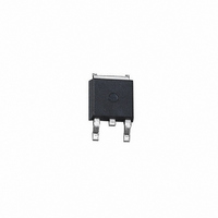
LP8345CDT-2.5/NOPB National Semiconductor, LP8345CDT-2.5/NOPB Datasheet - Page 6

LP8345CDT-2.5/NOPB
Manufacturer Part Number
LP8345CDT-2.5/NOPB
Description
IC REG LDO CMOS 500MA 2.5V 3DPAK
Manufacturer
National Semiconductor
Datasheet
1.LP8345CDTX-2.5NOPB.pdf
(13 pages)
Specifications of LP8345CDT-2.5/NOPB
Regulator Topology
Positive Fixed
Voltage - Output
2.5V
Voltage - Input
Up to 10V
Voltage - Dropout (typical)
0.335V @ 500mA
Number Of Regulators
1
Current - Output
500mA
Operating Temperature
0°C ~ 125°C
Mounting Type
Surface Mount
Package / Case
TO-252-2, DPak (2 Leads + Tab), TO-252AA, SC-63
Lead Free Status / RoHS Status
Lead free / RoHS Compliant
Current - Limit (min)
-
Other names
*LP8345CDT-2.5
*LP8345CDT-2.5/NOPB
LP8345CDT-2.5
*LP8345CDT-2.5/NOPB
LP8345CDT-2.5
www.national.com
V
I
I
T
e
Symbol
Q
LIMIT
n
SD
LP8345I Electrical Characteristics
IN
Unless otherwise specified all limits guaranteed for V
the full operating temperature range of T
Note 1: Absolute Maximum ratings indicate limits beyond which damage may occur. Electrical specifications do not apply when operating the device outside of its
rated operating conditions.
Note 2: All voltages are with respect to the potential at the ground pin.
Note 3: Maximum Power dissipation for the device is calculated using the following equations:
where T
the LLP package is specifically dependant on the PCB trace area, trace material, and the number of layers and thermal vias. For improved thermal resistance and
power dissipation for the LLP package, refer to Application Note AN-1187.
Note 4: Typical Values represent the most likely parametric norm.
Note 5: All limits are guaranteed by testing or statistical analysis.
Note 6: Human body model 1.5kΩ in series with 100pF.
Note 7: Condition does not apply to input voltages below 2.7V since this is the minimum input operating voltage.
Note 8: Dropout voltage is measured by reducing V
− V
O
J(MAX)
Dropout Voltage
(Note 7) (Note 8)
Quiescent Current
Minimum Load Current
Foldback Current Limit
Ripple Rejection Ratio
Thermal Shutdown
Temp.
Thermal Shutdown Hyst.
ADJ Input Leakage
Current
V
Output Noise
OUT
is the maximum junction temperature, T
Leakage Current
Parameter
LP8345-2.5
I
LP8345-3.3
LP8345-ADJ, V
LP8345-5.0
I
V
V
V
V
V
V
V
LP8345-ADJ
ADJ = OUT, V
LP8345-1.8, V
LP8345-2.5, V
LP8345-3.3, V
LP8345-5.0, V
10Hz to 10kHz, R
OUT
OUT
IN
IN
IN
IN
IN
IN
ADJ
≤10V
− V
− V
− V
(dc) = V
(ac) = 1V
J
= 500mA
= 500mA
IN
= 1.5V or 0V
= −40˚C to 125˚C
A
until V
OUT
OUT
OUT
is the ambient temperature, and θ
≤4V
>
<
OUT
O
P-P
5V
4V
drops 100mV from its normal value.
OUT
OUT
OUT
OUT
OUT
OUT
+ 2V
@
IN
Conditions
L
= 4V, V
= 6V, V
= 2.5V, V
= 3.5V, V
= 2V, V
120Hz
= 1kΩ, C
= V
= 3.3V, I
(Continued)
O
+ 1V, C
IN
IN
IN
6
IN
IN
OUT
OUT
= 10V
= 10V
= 10V
= 10V
= 10V
IN
= 500mA
= 10µF
JA
= C
is the junction-to-ambient thermal resistance. The value of the θ
OUT
= 10µF, T
(Note 5)
Min
48
J
= 25˚C. Boldface limits apply over
(Note 4)
±
1200
Typ
335
270
210
450
160
250
0.01
19
55
10
(Note 5)
±
Max
650
500
400
100
50
10
10
10
10
10
100
µVrms
Units
mV
mA
µA
µA
dB
nA
µA
JA
˚C
for


