LP8345CDT-3.3/NOPB National Semiconductor, LP8345CDT-3.3/NOPB Datasheet - Page 10
LP8345CDT-3.3/NOPB
Manufacturer Part Number
LP8345CDT-3.3/NOPB
Description
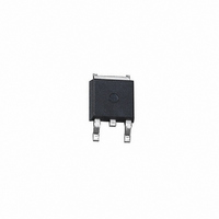
IC REG LDO CMOS 500MA 3.3V 3DPAK
Manufacturer
National Semiconductor
Datasheet
1.LP8345CDTX-2.5NOPB.pdf
(13 pages)
Specifications of LP8345CDT-3.3/NOPB
Regulator Topology
Positive Fixed
Voltage - Output
3.3V
Voltage - Input
Up to 10V
Voltage - Dropout (typical)
0.27V @ 500mA
Number Of Regulators
1
Current - Output
500mA
Operating Temperature
0°C ~ 125°C
Mounting Type
Surface Mount
Package / Case
TO-252-2, DPak (2 Leads + Tab), TO-252AA, SC-63
Lead Free Status / RoHS Status
Lead free / RoHS Compliant
Current - Limit (min)
-
Other names
*LP8345CDT-3.3
*LP8345CDT-3.3/NOPB
LP8345CDT-3.3
*LP8345CDT-3.3/NOPB
LP8345CDT-3.3


www.national.com
Applications Section
GENERAL INFORMATION
The LP8345 is a low-dropout, low quiescent current linear
regulator. As shown in Figure 1 it consists of a 1.25V refer-
ence, error amplifier, MOSFET driver, PMOS pass transistor
and for the fixed output versions, an internal feedback net-
work (R
load by a thermal shutdown circuit and a foldback current
limit circuit.
The 1.25V reference is connected to the inverting input of
the error amplifier. Regulation of the output voltage is
EXTERNAL CAPACITOR
An Input capacitor of 1µF or greater is required between the
LP8345 V
bypassing of the V
(i.e. 10µF) can provide improved bypassing of power supply
noise.
Stable operation can be achieved with an output capacitor of
1µF or greater, either ceramic X7R dielectric or aluminum/
tantalum electrolytic. While the minimum capacitor value is
1µF, the typical output capacitor values selected range from
1µF to 10µF. The larger values provide improved load-
transient response, power supply rejection and stability.
OUTPUT VOLTAGE SETTING (ADJ VERSION ONLY)
The output voltage is set according to the amount of nega-
tive feedback (Note that the pass transistor inverts the feed-
back signal). This feedback is determined by R
the resulting output voltage represented by the following
equation:
1
/R
IN
2
). In addition, the device is protected from over-
pin and ground. While 1µF will provide adequate
IN
supply larger values of input capacitor
FIGURE 1. LP8345 Functional Block Diagram
1
and R
2
with
10
achieved by means of negative feedback to the non-
inverting input of the error amplifier. Feedback resistors R
and R
ing on whether it is a fixed voltage version or the adjustable
version. The negative feedback and high open loop gain of
the error amplifier cause the two inputs of the error amp to be
virtually equal in voltage. If the output voltage changes due
to load changes, the error amplifier and MOSFET driver
provide the appropriate drive to the pass transistor to main-
tain the error amplifier’s inputs as virtually equal.
Use the following equation to determine the values of R
R
MINIMUM LOAD CURRENT
A minimum load of 100µA is required for regulation and
stability over the entire operating temperature range. If ac-
tual load current fall below 100µA it is recommended that a
resistor of value R
ground.
2
for a desired V
2
are either internal or external to the device, depend-
OUT
L
=V
(R
O
/100µA be placed between V
2
= 100kΩ is recommended).
20064803
O
1
and
and
1
Related parts for LP8345CDT-3.3/NOPB
Image
Part Number
Description
Manufacturer
Datasheet
Request
R

Part Number:
Description:
IC REG LDO CMOS 500MA 5V 3-DPAK
Manufacturer:
National Semiconductor
Datasheet:
Part Number:
Description:
IC REG LDO CMOS 500MA 1.8V 3DPAK
Manufacturer:
National Semiconductor
Datasheet:
Part Number:
Description:
IC REG LDO CMOS 500MA 2.5V 3DPAK
Manufacturer:
National Semiconductor
Datasheet:

Part Number:
Description:
Low Dropout, Low IQ, 500mA CMOS Linear Regulator
Manufacturer:
NSC [National Semiconductor]
Datasheet:

Part Number:
Description:
National Semiconductor [8-Bit D/A Converter]
Manufacturer:
National Semiconductor
Datasheet:
Part Number:
Description:
National Semiconductor [Media Coprocessor]
Manufacturer:
National Semiconductor
Datasheet:
Part Number:
Description:
Digitally Controlled Tone and Volume Circuit with Stereo Audio Power Amplifier, Microphone Preamp Stage and National 3D Sound
Manufacturer:
National Semiconductor
Datasheet:
Part Number:
Description:
Digitally Controlled Tone and Volume Circuit with Stereo Audio Power Amplifier, Microphone Preamp Stage and National 3D Sound
Manufacturer:
National Semiconductor
Datasheet:
Part Number:
Description:
AC97 Rev 2 Codec with Sample Rate Conversion and National 3D Sound
Manufacturer:
National Semiconductor
Part Number:
Description:
Manufacturer:
National Semiconductor
Datasheet:
Part Number:
Description:
Manufacturer:
National Semiconductor
Datasheet:
Part Number:
Description:
General Purpose, Low Voltage, Low Power, Rail-to-Rail Output Operational Amplifiers
Manufacturer:
National Semiconductor
Datasheet:
Part Number:
Description:
8-bit 20 MSPS flash A/D converter.
Manufacturer:
National Semiconductor
Datasheet:
Part Number:
Description:
Low Noise Quad Operational Amplifier
Manufacturer:
National Semiconductor
Datasheet: