EVAL6229QR STMicroelectronics, EVAL6229QR Datasheet - Page 20
EVAL6229QR
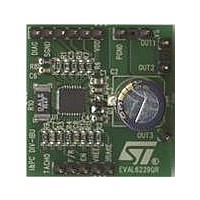
Manufacturer Part Number
EVAL6229QR
Description
BOARD DEMO L6229Q BLDC MOT CTRL
Manufacturer
STMicroelectronics
Type
Motor / Motion Controllers & Driversr
Specifications of EVAL6229QR
Main Purpose
Power Management, Motor Control
Embedded
No
Utilized Ic / Part
L6229Q
Primary Attributes
3-Ph BLDC, 8 ~ 52V Output, PWM Current Control, Brake Function
Secondary Attributes
Over Current, Cross Conduction & Temperature Protection
Maximum Operating Temperature
+ 125 C
Operating Supply Voltage
8 V to 52 V
Product
Power Management Development Tools
Lead Free Status / RoHS Status
Lead free / RoHS Compliant
For Use With/related Products
L6229Q
Other names
497-10748


Circuit description
5.7
20/28
Non-dissipative overcurrent detection and protection
The L6229Q integrates an overcurrent detection circuit (OCD) for full protection. This circuit
provides output-to-output and output-to-ground short circuit protection as well. With this
internal over current detection, the external current sense resistor normally used and its
associated power dissipation are eliminated.
overcurrent detection circuit.
To implement the over current detection, a sensing element that delivers a small but precise
fraction of the output current is implemented with each high side power MOS. Since this
current is a small fraction of the output current there is very little additional power
dissipation. This current is compared with an internal reference current I
output current reaches the detection threshold (typically I
comparator signals a fault condition. When a fault condition is detected, an internal open
drain MOS with a pull down capability of 4 mA connected to pin DIAG is turned on.
The pin DIAG can be used to signal the fault condition to a μC or to shut down the three-
phase bridge simply by connecting it to pin EN and adding an external R-C (see R
Figure 19. Overcurrent protection simplified schematic
Figure 20
recovering normal operation can be easily programmed by means of the accurate
thresholds of the logic inputs. It is affected whether by C
magnitude is reported in
an overcurrent has been detected depends only by C
Figure 22
C
the value of C
delay time and the R
The resistor R
values for R
disable time.
EN
μC or LOGIC
V
DD
is also used for providing immunity to pin EN against fast transient noises. Therefore
R
C
EN
EN
shows the overcurrent detection operation. The disable time t
EN
EN
DIAG
EN
and C
EN
should be chosen as big as possible according to the maximum tolerable
should be chosen in the range from 2.2 kΩ to 180 kΩ. Recommended
TO GATE
40Ω TYP.
R
LOGIC
DS(ON)
EN
EN
POWER SENSE
value should be chosen according to the desired disable time.
are respectively 100 kΩ and 5.6 nF that allow obtaining 200 μs
Figure
OPEN-DRAIN
INTERNAL
1 cell
COMPARATOR
Doc ID 15209 Rev 3
OCD
21. The delay time t
HIGH SIDE DMOS
POWER DMOS
OVER TEMPERATURE
n cells
I
1
OUT
I
1
/ n
1
I
I
I
REF
REF
1
+I
Figure 19
VS
2
+
/ n
A
OUT
I
2
DELAY
/ n
2
POWER DMOS
HIGH SIDE DMOS
I
2
EN
n cells
shows a simplified schematic for the
EN
value. Its magnitude is reported in
SOVER
before turning off the bridge when
and R
D02IN1381
POWER SENSE
I
= 2.8 A) the OCD
3
1 cell
/ n
EN
values and its
OUT
DISABLE
3
POWER DMOS
REF
I
3
VS
n cells
. When the
B
HIGH SIDE DMOS
before
POWER SENSE
EN
L6229Q
, C
1 cell
EN
).
Related parts for EVAL6229QR
Image
Part Number
Description
Manufacturer
Datasheet
Request
R

Part Number:
Description:
ENERCHIP CC EVAL KIT
Manufacturer:
Cymbet Corporation
Datasheet:

Part Number:
Description:
BOARD EVAL FOR AD976
Manufacturer:
Analog Devices Inc
Datasheet:

Part Number:
Description:
BOARD EVAL FOR ADXL345
Manufacturer:
Analog Devices Inc
Datasheet:

Part Number:
Description:
ENERCHIP CC SEH EVAL KIT
Manufacturer:
Cymbet Corporation
Datasheet:

Part Number:
Description:
ENERCHIP EP ENERGY HARVEST EVAL
Manufacturer:
Cymbet Corporation
Datasheet:

Part Number:
Description:
EVAL BOARD FOR TW6864-LB2-GR
Manufacturer:
Intersil
Datasheet:
Part Number:
Description:
EVAL BOARD FOR TW8816-LB3-GR
Manufacturer:
Intersil
Datasheet:
Part Number:
Description:
EVAL BOARD FOR TW8817-TA3-GRS
Manufacturer:
Intersil
Datasheet:

Part Number:
Description:
EVALUATION MODULE FOR ADUM4160
Manufacturer:
Analog Devices Inc
Datasheet:

Part Number:
Description:
BOARD EVALUATION ADCMP581BCP
Manufacturer:
Analog Devices Inc
Datasheet:
Part Number:
Description:
BOARD EVALUATION ADM1041
Manufacturer:
Analog Devices Inc
Datasheet:

Part Number:
Description:
EVAL BOARD FOR STM32F107VCT
Manufacturer:
STMicroelectronics
Datasheet:
Part Number:
Description:
BOARD EVAL FOR AD1954
Manufacturer:
Analog Devices Inc
Datasheet:
Part Number:
Description:
BOARD EVAL FOR AD1955
Manufacturer:
Analog Devices Inc
Datasheet:

Part Number:
Description:
BOARD EVAL FOR AD7655
Manufacturer:
Analog Devices Inc
Datasheet: