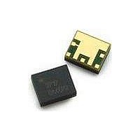
ALM-2712-BLKG Avago Technologies US Inc., ALM-2712-BLKG Datasheet
ALM-2712-BLKG
Specifications of ALM-2712-BLKG


Related parts for ALM-2712-BLKG


ALM-2712-BLKG Summary of contents
Page 1
... ALM-2712 GPS Filter-LNA-Filter Front-End Module Data Sheet Description Avago Technologies’ ALM-2712 is an ultra low-noise GPS front-end module that combines a low-noise amplifier (LNA) with GPS FBAR filters. The LNA uses Avago Tech- nologies’ proprietary GaAs Enhancement-mode pHEMT process to achieve high gain with very low noise figure and high linearity ...
Page 2
Absolute Maximum Rating T =25°C A Symbol Parameter Vdd Device Drain to Source Voltage [2] Idd Drain Current Input Power (Vdd = 2.7V, Idd = 7.5mA) in,max [4] P Total Power Dissipation diss T Junction Temperature ...
Page 3
Electrical Specifications T = 25°C, Freq = 1.575GHz, measured on demo board A Table 1. Performance at Vdd = Vsd = 2.7V, Idd = 7.5mA (Rbias = 6.8k Ohm) nominal operating conditions Symbol Parameter and Test Condition G Gain [2] ...
Page 4
Table 2. Performance at Vdd = Vsd = 1.8V, Idd = 5mA (Rbias = 2.7k Ohm) nominal operating conditions Symbol Parameter and Test Condition G Gain [2] NF Noise Figure IP1dB Input 1dB Compressed Power [3] rd IIP3 Input 3 ...
Page 5
Avago Tech DC Pin Configuration of 4-Pins connector Pins pointing out of the page Circuit Symbol Size Description L1 0402 22 nH Inductor (Taiyo Yuden HK100522NJ-T) C1 0805 0.1 uF Capacitor (Murata GRM21BR71H104KA01L) C2 0402 47 pF Capacitor (Kyocera CM05CH470J50AHF) ...
Page 6
Vsd C3* R2* RFin Figure 8. Application Circuit * optional, see notes below Notes x The module is fully matched at the input and output RF pins. The RFinput pin is connected directly to a shunt inductor to ground. As ...
Page 7
... ALM-2712 Typical Performance Curves at 25° -20 -40 WLAN band High band Low band -60 -80 -100 0.0 0.4 0.8 1.2 1.6 2.0 2.4 Freq (GHz) Figure 9a. Typical S-Parameter Plot @ Vdd = 2.7V, Idd = 7.5mA -65 -70 -75 -80 -85 0.8 Freq (GHz) Figure 9c. Rejection plot for Low band @ Vdd = 2.7V, Idd = 7.5mA ...
Page 8
... ALM-2712 Typical Performance Curves at 25° -20 -40 -60 -80 -100 0.0 0.4 0.8 1.2 1.6 2.0 2.4 Freq (GHz) Figure 10a. Typical S-Parameter Plot @ Vdd = 1.8V, Idd = 5mA Rbias (kohm) Figure 11. Idd vs Rbias at 25° 0.5 1 1.5 Vsd (V) Figure 13. Idd vs Vsd for Vdd = 1.8V 2.7k Ohm ...
Page 9
... ALM-2712 Typical Performance Curves 2.6 2.4 2.2 2.0 1.8 1.6 1.4 1.2 1.0 0 Idd (mA) Figure 14. NF vs. Idd at Vdd = 2. Idd (mA) Figure 16. Gain vs. Idd at Vdd = 2.7V -65 -70 -75 -80 -85 -90 - Idd (mA) Figure 18. Low band rejection vs. Idd at Vdd = 2.7V 9 2.6 -40°C 2.4 25°C 2.2 85°C 2 ...
Page 10
... ALM-2712 Typical Performance Curves -65 -70 -75 -80 -85 -90 - Idd (mA) Figure 20. High band rejection vs. Idd at Vdd = 2.7V -65 -70 -75 -80 -85 -90 - Idd (mA) Figure 22. WLAN band rejection vs. Idd at Vdd = 2. 1.8 2.0 2.2 2.4 2.6 2.8 Vdd (V) Figure 24. IP1dB vs. Vdd at 25°C 10 -65 -40°C 25°C -70 85°C ...
Page 11
... ALM-2712 Typical Performance Curves at 25° 2.0 1.8 1.6 1.4 1.2 1.0 0 freq, GHz Figure 26. Edwards-Sinsky Output Stability Factor (Mu) at Vdd = 2.7V 2.0 1.8 1.6 1.4 1.2 1.0 0 freq, GHz Figure 28. Edwards-Sinsky Output Stability Factor (Mu) at Vdd = 1.8V 11 2.0 1.8 1.6 1 ...
Page 12
... ALM-2712 module with differential output A differential output can be implemented for the ALM-2712 using the schematic shown below. Suggested component values are listed in Table 3. C1, C2 and L1, L2 are to convert the single-ended output to differential outputs while C3, C4 and L3 provide matching to 100 ohm differential impedance. ...
Page 13
... ALM-2712 Scattering Parameter and Measurement Reference Planes GPS FILTER REFERENCE PLANE Figure 31. Scattering parameter measurement reference planes LNA 8 GPS FILTER 11 R2 MODULE C3 REFERENCE PLANE ...
Page 14
... ALM-2712 Typical Scattering Parameters at 25°C, Vdd = 2.7V, Idd = 7.5mA The S- and Noise Parameters are measured using a coplanar waveguide PCB with 10 mils Rogers shows the input and output reference planes. The circuit values are as indicated in Figure 7. Freq S11 S11 (GHz) Mag.(dB) Ang ...
Page 15
... ALM-2712 Typical Scattering Parameters at 25°C, Vdd = 1.8V, Idd = 5mA S11 S11 Freq (GHz) Mag.(dB) Ang. 0.05 -0.31 170.81 0.1 -0.45 162.64 0.2 -0.61 146.96 0.3 -0.69 131.53 0.4 -0.63 116.79 0.5 -0.65 101.24 0.6 -0.67 85.55 0.7 -0.69 69.56 0.8 -0 ...
Page 16
... The exceptional noise figure performance of the ALM-2712 is due to its highly optimized design. In this regard, the Fmin of the ALM-2712 shown above is locked down by the internal input pre-match. This allows the use of relatively inexpensive chip inductors for external matching. Part Number Ordering Information Part Number Qty ALM-2712-BLKG 100 ALM-2712-TR1G 3000 ALM-2712-SG1G ...
Page 17
PCB Land Patterns and Stencil Design 2.80 2.50 1.25 0.60 0.90 1.60 2.80 Land Pattern 2.50 1.25 0.90 1.53 1.60 2.52 2.80 Combination of Land Pattern and Stencil Opening Notes: 1. All dimensions are in milimeters 2. Recommended stencil thickness ...
Page 18
Device Orientation REEL USER FEED COVER TAPE DIRECTION Tape Dimensions 2.00 ± .05 SEE NOTE 3 4.00 SEE NOTE 1 0.30 ± .05 R 0.30 MAX SECTION A – A Notes: 1. All dimensions ...
Page 19
Reel Dimensions (7” reel) 6.25mm Embossed Letters Lettering Thickness 1.6mm Slot Hole (2X) 180° Apart Recycle Logo FRONT VIEW BACK VIEW 19 ø178.0 ± 0.5 See Detail “X” FRONT See Detail “Y” 1.5 Min +0.5 ø13.0 0.2 ø20.2 Min Detail ...
Page 20
Reel Dimensions (13” reel DATE CODE EMBOSSED LETTERING 7.5mm HEIGHT EMBOSSED LINE (2x) 89.0mm LENGTH LINES 147.0mm AWAY FROM CENTER POINT ESD LOGO 6 PS RECYCLE LOGO SEE ...