AD8312ACBZ-P7 Analog Devices Inc, AD8312ACBZ-P7 Datasheet - Page 7
AD8312ACBZ-P7
Manufacturer Part Number
AD8312ACBZ-P7
Description
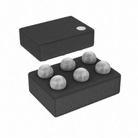
IC DETECTOR RF LOGIC 6-WLCSP
Manufacturer
Analog Devices Inc
Type
Logarithmic Amplifierr
Datasheet
1.AD8312ACBZ-P7.pdf
(20 pages)
Specifications of AD8312ACBZ-P7
Rf Type
Cellular, GSM, CDMA, W-CDMA
Frequency
50MHz ~ 3.5GHz
Input Range
-45dBm ~ 0dBm
Accuracy
±1dB
Voltage - Supply
2.7 V ~ 5.5 V
Current - Supply
5.7mA
Package / Case
6-UFBGA, 6-uCSP
Frequency Range
50MHz To 3.5GHz
Power Range
-45dBm To 0dBm
Sensitivity
0.0073dB/°C
Supply Current
4.2mA
Supply Voltage Range
2.7V To 5.5V
Rf Ic Case Style
WLCSP
Number Of Channels
1
Number Of Elements
1
Power Supply Requirement
Single
Input Resistance
0.013MOhm
Input Bias Current
75uA
Single Supply Voltage (typ)
3V
Dual Supply Voltage (typ)
Not RequiredV
Power Dissipation
200mW
Rail/rail I/o Type
No
Single Supply Voltage (min)
2.7V
Single Supply Voltage (max)
5.5V
Dual Supply Voltage (min)
Not RequiredV
Dual Supply Voltage (max)
Not RequiredV
Operating Temp Range
-40C to 85C
Operating Temperature Classification
Industrial
Mounting
Surface Mount
Pin Count
6
Package Type
WLCSP
Lead Free Status / RoHS Status
Lead free / RoHS Compliant
Lead Free Status / RoHS Status
Lead free / RoHS Compliant, Lead free / RoHS Compliant
Other names
AD8312ACBZ-P7
AD8312ACBZ-P7TR
AD8312ACBZ-P7TR
Available stocks
Company
Part Number
Manufacturer
Quantity
Price
Company:

Part Number:
AD8312ACBZ-P7
Manufacturer:
ADI
Quantity:
9 000
Company:
Part Number:
AD8312ACBZ-P7
Manufacturer:
ST
Quantity:
320


PIN CONFIGURATION AND FUNCTION DESCRIPTIONS
Table 3. Pin Function Descriptions
Ball No.
1
2
3
4
5
6
Mnemonic
VPOS
VOUT
VSET
CFLT
COMM
RFIN
Description
Positive Supply Voltage (V
Logarithmic Output. Output voltage increases with increasing input amplitude.
Setpoint Input. Connect VSET to VOUT for measurement-mode operation. The nominal logarithmic slope of
20 mV/dB can be increased to an arbitrarily high value by attenuating the signal between VOUT and VSET
(see the Increasing the Logarithmic Slope section).
Connection for an External Capacitor to Slow the Response of the Output. Capacitor is connected between
CFLT and VOUT.
Device Common (Ground).
RF Input.
S
), 2.7 V to 5.5 V.
VPOS
VOUT
VSET
Figure 2. Pin Configuration
Rev. A | Page 7 of 20
(Not to Scale)
AD8312
TOP VIEW
1
2
3
6
5
4
RFIN
COMM
CFLT
AD8312
Related parts for AD8312ACBZ-P7
Image
Part Number
Description
Manufacturer
Datasheet
Request
R

Part Number:
Description:
High-Performance, Low Distortion 500-MHz Mixer
Manufacturer:
Analog Devices
Datasheet:

Part Number:
Description:
MIXER IC
Manufacturer:
Analog Devices Inc
Datasheet:
Part Number:
Description:
MIXER IC
Manufacturer:
Analog Devices Inc
Datasheet:

Part Number:
Description:
±1.7g Dual-Axis IMEMS Accelerometer Evaluation Board
Manufacturer:
Analog Devices Inc
Datasheet:

Part Number:
Description:
Inertial Sensor Evaluation System
Manufacturer:
Analog Devices Inc
Datasheet:
Part Number:
Description:
Manufacturer:
Analog Devices Inc
Datasheet:
Part Number:
Description:
Manufacturer:
Analog Devices Inc
Datasheet:
Part Number:
Description:
Manufacturer:
Analog Devices Inc
Datasheet:
Part Number:
Description:
Manufacturer:
Analog Devices Inc
Datasheet:
Part Number:
Description:
Manufacturer:
Analog Devices Inc
Datasheet:
Part Number:
Description:
Manufacturer:
Analog Devices Inc
Datasheet:
Part Number:
Description:
Manufacturer:
Analog Devices Inc
Datasheet: