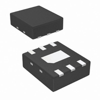
LMV221SDX/NOPB National Semiconductor, LMV221SDX/NOPB Datasheet - Page 23

LMV221SDX/NOPB
Manufacturer Part Number
LMV221SDX/NOPB
Description
IC RF DETECTOR CDMA/WCDMA 6-LLP
Manufacturer
National Semiconductor
Datasheet
1.LMV221SDNOPB.pdf
(32 pages)
Specifications of LMV221SDX/NOPB
Frequency
50MHz ~ 3.5GHz
Rf Type
Cellular, CDMA, CDMA2000, EDGE, GSM, GPRS, TDMA, W-CDMA
Input Range
-45dBm ~ 5dBm
Accuracy
0.5dB
Voltage - Supply
2.7 V ~ 3.3 V
Current - Supply
10mA
Package / Case
6-LLP
Lead Free Status / RoHS Status
Lead free / RoHS Compliant
Other names
LMV221SDX
Available stocks
Company
Part Number
Manufacturer
Quantity
Price
Part Number:
LMV221SDX/NOPB
Manufacturer:
NS/国半
Quantity:
20 000
Unfortunately, the (numeric) inverse of the detector transfer
function at different temperatures makes this expression
rather impractical. However, since the drift error is usually
small V
means that we can apply the following approximation:
This expression is easily simplified by taking the following
considerations into account:
•
•
•
•
Using this, we arrive at:
This expression is very similar to the expression of the LOG-
conformance error determined previously. The only differ-
ence is that instead of the output of the ideal LOG-linear
model, the actual detector output voltage at the calibration
temperature is now subtracted from the detector output volt-
age at the operating temperature.
Figure 7 depicts an example of the drift error.
The drift error at the calibration temperature E(T
equals zero (by definition).
The estimator transfer F
temperature; the estimator output changes over
temperature only due to the temperature dependence of
V
The actual detector input power P
dependent (in the context of this expression).
The derivative of the estimator transfer function to V
equals approximately 1/K
the detector transfer function (the region of interest).
FIGURE 7. Temperature Drift Error of the LMV221
OUT
OUT
.
(T) is only slightly different from V
at f = 1855 MHz
DET
SLOPE
(V
OUT
in the LOG-linear region of
,T
IN
O
is not temperature
) is not a function of
OUT
20173722
(T
O
O
,T
). This
O
OUT
)
23
In agreement with the definition, the temperature drift error is
zero at the calibration temperature. Further, the main differ-
ence with the LOG-conformance error is observed at the top
and bottom end of the detection range; instead of a rapid in-
crease the drift error settles to a small value at high and low
input power levels due to the fact that the detector saturation
levels are relatively temperature independent.
In a practical application it may not be possible to use the
exact inverse detector transfer function as the algorithm for
the estimator. For example it may require too much memory
and/or too much factory calibration time. However, using the
ideal LOG-linear model in combination with a few extra data
points at the top and bottom end of the detection range -
where the deviation is largest - can already significantly re-
duce the power measurement error.
2.4 Temperature Compensation
A further reduction of the power measurement error is possi-
ble if the operating temperature is measured in the applica-
tion. For this purpose, the detector model used by the
estimator should be extended to cover the temperature de-
pendency of the detector.
Since the detector transfer function is generally a smooth
function of temperature (the output voltage changes gradually
over temperature), the temperature is in most cases ade-
quately modeled by a first-order or second-order polynomial,
i.e.
The required temperature dependence of the estimator, to
compensate for the detector temperature dependence can be
approximated similarly:
The last approximation results from the fact that a first-order
temperature compensation is usually sufficiently accurate.
The remainder of this section will therefore concentrate on
first-order compensation. For second and higher-order com-
pensation a similar approach can be followed.
Ideally, the temperature drift could be completely eliminated
if the measurement system is calibrated at various tempera-
tures and input power levels to determine the Temperature
Sensitivity S
ally not possible due to the associated high costs. The alter-
native is to use the average temperature drift in the estimator,
instead of the temperature sensitivity of each device individ-
ually. In this way it becomes possible to eliminate the sys-
tematic (reproducible) component of the temperature drift
without the need for calibration at different temperatures dur-
ing manufacturing. What remains is the random temperature
drift, which differs from device to device. Figure 8 illustrates
the idea. The graph at the left schematically represents the
behavior of the drift error versus temperature at a certain input
power level for a large number of devices.
1
. In a practical application, however that is usu-
www.national.com


