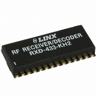
RXD-433-KH2 Linx Technologies Inc, RXD-433-KH2 Datasheet - Page 5
RXD-433-KH2
Manufacturer Part Number
RXD-433-KH2
Description
RECEIVER/DECODER 433MHZ KH2 SER
Manufacturer
Linx Technologies Inc
Series
KH2r
Datasheet
1.RXD-418-KH2.pdf
(11 pages)
Specifications of RXD-433-KH2
Frequency
433MHz
Sensitivity
-102dBm
Data Rate - Maximum
5 kbps
Modulation Or Protocol
ASK, OOK
Applications
Garage Openers, RKE, Security Alarms
Current - Receiving
5mA
Data Interface
PCB, Surface Mount
Antenna Connector
PCB, Surface Mount
Features
Built-in Remote Control Decoder
Voltage - Supply
2.7 V ~ 3.6 V
Operating Temperature
-40°C ~ 70°C
Package / Case
Non-Standard SMD
Board Size
36.3 mm x 16 mm x 4.6 mm
Minimum Operating Temperature
- 40 C
Supply Voltage (min)
2.7 V
Product
RF Modules
Maximum Frequency
433.92 MHz
Supply Voltage (max)
3.6 V
Maximum Operating Temperature
+ 70 C
Lead Free Status / RoHS Status
Lead free / RoHS Compliant
Memory Size
-
Lead Free Status / Rohs Status
Lead free / RoHS Compliant
Available stocks
Company
Part Number
Manufacturer
Quantity
Price
Company:

Part Number:
RXD-433-KH2
Manufacturer:
LNX
Quantity:
100


USING THE RSSI PIN
INTERFERENCE CONSIDERATIONS
Page 8
The receiver’s Received Signal Strength Indicator (RSSI) line serves a variety of
functions. This line has a dynamic range of 80dB (typical) and outputs a voltage
proportional to the incoming signal strength. It should be noted that the RSSI
levels and dynamic range will vary slightly from part to part. It is also important
to remember that RSSI output indicates the strength of any in-band RF energy
and not necessarily just that from the intended transmitter; therefore, it should be
used only to qualify the level and presence of a signal.
The RSSI output can be utilized during testing or even as a product feature to
assess interference and channel quality by looking at the RSSI level with all
intended transmitters shut off. The RSSI output can also be used in direction-
finding applications, although there are many potential perils to consider in such
systems. Finally, it can be used to save system power by “waking up” external
circuitry when a transmission is received or crosses a certain threshold. The
RSSI output feature adds tremendous versatility for the creative designer.
The RF spectrum is crowded and the potential for conflict with other unwanted
sources of RF is very real. While all RF products are at risk from interference, its
effects can be minimized by better understanding its characteristics.
Interference may come from internal or external sources. The first step is to
eliminate interference from noise sources on the board. This means paying
careful attention to layout, grounding, filtering, and bypassing in order to
eliminate all radiated and conducted interference paths. For many products, this
is straightforward; however, products containing components such as switching
power supplies, motors, crystals, and other potential sources of noise must be
approached with care. Comparing your own design with a Linx evaluation board
can help to determine if and at what level design-specific interference is present.
External interference can manifest itself in a variety of ways. Low-level
interference will produce noise and hashing on the output and reduce the link’s
overall range.
High-level interference is caused by nearby products sharing the same
frequency or from near-band high-power devices. It can even come from your
own products if more than one transmitter is active in the same area. It is
important to remember that only one transmitter at a time can occupy a
frequency, regardless of the coding of the transmitted signal. This type of
interference is less common than those mentioned previously, but in severe
cases it can prevent all useful function of the affected device.
Although technically it is not interference, multipath is also a factor to be
understood. Multipath is a term used to refer to the signal cancellation effects
that occur when RF waves arrive at the receiver in different phase relationships.
This effect is a particularly significant factor in interior environments where
objects provide many different signal reflection paths. Multipath cancellation
results in lowered signal levels at the receiver and, thus, shorter useful distances
for the link.
TYPICAL APPLICATIONS
Figure 12: Basic Remote Control Receiver
GND
VCC
The figure below shows an example of a basic remote control receiver utilizing
the KH2 Series receiver module. When a key is pressed on the transmitter, a
corresponding line on the receiver goes high. A schematic for the transmitter /
encoder circuit may be found in the KH Series Transmitter Data Guide. These
circuits are implemented in the KH Series Basic Evaluation Kit. They can be
easily modified for a custom application and clearly demonstrate the ease of
using the Linx KH Series modules for remote control applications.
The ten-position DIP switch is used to set the address to either ground or
floating. Since the floating state is a valid state, no pull-up resistors are needed.
The data line outputs can only source about 1mA of current, so transistor buffers
are used to drive the buzzer and LED. 1mA is sufficient to activate most
microcontrollers, but the manufacturer’s data guides should be consulted to
make sure.
The KH2 Series receiver / decoder module is also suitable for use with Linx OEM
handheld transmitters. These transmitters are FCC certified, making product
introduction extremely quick. Information on these transmitters can be found on
the Linx website at www.linxtechnologies.com.
R4
10k
Q1
2N2222
Figure 13: Linx OEM Transmitters
VCC
GND
BZ1
BUZZER
R6
220 OHM
R5
10k
LED1
RED LED
Q2
2N2222
R2
2.2k
R3
2.2k
VCC
GND
10
11
12
13
14
1
2
3
4
5
6
7
8
9
RXD-XXX-KH2
NC
D0
D1
GND
VCC
PDN
D2
D3
D4
DATA
VT
D5
D6
D7
RSSI
GND
ANT
Figure 14: Linx OEM Keyfobs
NC
A9
A8
A7
A6
A5
A4
A3
A2
A1
A0
28
27
26
25
24
23
22
21
20
19
18
17
16
15
ANT1
GND
VCC
GND
10
S4
1
2
3
4
5
6
7
8
9
B1
CR2032 3V LITHIUM
S1
SW-DIP-10
20
19
18
17
16
15
14
13
12
11
GND
Page 9
Related parts for RXD-433-KH2
Image
Part Number
Description
Manufacturer
Datasheet
Request
R

Part Number:
Description:
RECEIVER RF 433MHZ SMT
Manufacturer:
Linx Technologies Inc
Datasheet:

Part Number:
Description:
RECEIVER RF 418MHZ SMT KH2 SER
Manufacturer:
Linx Technologies Inc
Datasheet:

Part Number:
Description:
RECEIVER RF 315MHZ SMT KH2 SER
Manufacturer:
Linx Technologies Inc
Datasheet:

Part Number:
Description:
RECEIVER RF 315MHZ SMT
Manufacturer:
Linx Technologies Inc
Datasheet:
Part Number:
Description:
RECEIVER RF 418MHZ SMT
Manufacturer:
Linx Technologies Inc
Datasheet:

Part Number:
Description:
HOLDER BATTERY 20MM COIN CR2032
Manufacturer:
Linx Technologies Inc
Datasheet:

Part Number:
Description:
CONN RPSMA BL CRJA-CPV 8.5" COAX
Manufacturer:
Linx Technologies Inc

Part Number:
Description:
CABLE RG174 RPSMA M/F 8.5"
Manufacturer:
Linx Technologies Inc

Part Number:
Description:
CABLE RG174 SMA M/F 8.5"
Manufacturer:
Linx Technologies Inc

Part Number:
Description:
CABLE RPSMA/SMA 8.5"
Manufacturer:
Linx Technologies Inc

Part Number:
Description:
MODULE USB LOW SPEED
Manufacturer:
Linx Technologies Inc
Datasheet:

Part Number:
Description:
IC TRANSCODER MT BI-DIR 20-SSOP
Manufacturer:
Linx Technologies Inc
Datasheet:

Part Number:
Description:
IC ENCODER LOW SECURITY 8DIP
Manufacturer:
Linx Technologies Inc
Datasheet:

Part Number:
Description:
IC DECODER MS SERIES 20-SSOP
Manufacturer:
Linx Technologies Inc
Datasheet:
Part Number:
Description:
IC ENCODER MS SERIES 20-SSOP
Manufacturer:
Linx Technologies Inc
Datasheet: