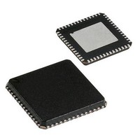
CYRF69103-40LFXC Cypress Semiconductor Corp, CYRF69103-40LFXC Datasheet - Page 20

CYRF69103-40LFXC
Manufacturer Part Number
CYRF69103-40LFXC
Description
IC PROC 8K FLASH 40VQFN
Manufacturer
Cypress Semiconductor Corp
Series
CYRFr
Datasheet
1.CYRF69103-40LFXC.pdf
(68 pages)
Specifications of CYRF69103-40LFXC
Package / Case
40-VQFN Exposed Pad, 40-HVQFN, 40-SQFN, 40-DHVQFN
Frequency
2.4GHz
Data Rate - Maximum
1Mbps
Modulation Or Protocol
ISM
Applications
General Purpose
Power - Output
6dBm
Sensitivity
-87dBm
Voltage - Supply
1.8 V ~ 3.6 V
Current - Receiving
21.9mA
Current - Transmitting
39.9mA
Data Interface
PCB, Surface Mount
Memory Size
8kB Flash, 256B SRAM
Antenna Connector
PCB, Surface Mount
Operating Temperature
0°C ~ 70°C
Processor Series
CYRF691x
Core
M8C
Data Bus Width
8 bit
Data Ram Size
256 B
Interface Type
SPI
Maximum Clock Frequency
2 MHz
Number Of Programmable I/os
15
Number Of Timers
4
Operating Supply Voltage
2.5 V, 3.3 V
Maximum Operating Temperature
+ 70 C
Mounting Style
SMD/SMT
Minimum Operating Temperature
0 C
Program Memory Type
Flash
Program Memory Size
8 KB
Operating Temperature (min)
0C
Operating Temperature (max)
70C
Operating Temperature Classification
Commercial
Operating Supply Voltage (min)
1.8V
Operating Supply Voltage (typ)
2.5/3.3V
Operating Supply Voltage (max)
3.6V
Height
1 mm
Length
5.9 mm
Supply Voltage (max)
3.6 V
Supply Voltage (min)
1.8 V
Width
5.9 mm
Lead Free Status / RoHS Status
Lead free / RoHS Compliant
For Use With
770-1001 - ISP 4PORT CYPRESS ENCORE II MCU
Lead Free Status / Rohs Status
Lead free / RoHS Compliant
Other names
428-1933
Available stocks
Company
Part Number
Manufacturer
Quantity
Price
Part Number:
CYRF69103-40LFXC
Manufacturer:
CYCRESS
Quantity:
20 000
14.2 Data Memory Organization
The MCU function provides up to 256 bytes of data RAM.
14.3 Flash
This section describes the Flash block of the CYRF69103. Much
of the user visible Flash functionality, including programming and
security, are implemented in the M8C Supervisory Read Only
Memory (SROM). CYRF69103 Flash has an endurance of 1000
cycles and 10-year data retention.
14.3.1 Flash Programming and Security
All Flash programming is performed by code in the SROM. The
registers that control the Flash programming are only visible to
the M8C CPU when it is executing out of SROM. This makes it
impossible to read, write, or erase the Flash by bypassing the
security mechanisms implemented in the SROM.
Customer firmware can only program the Flash through SROM
calls. The data or code images can be sourced by way of any
interface with the appropriate support firmware. This type of
programming requires a ‘bootloader’—a piece of firmware
resident on the Flash. For safety reasons, this bootloader must
not be over written during firmware rewrites.
The Flash provides four auxiliary rows that are used to hold Flash
block protection flags, boot time calibration values, configuration
tables, and any device values. The routines for accessing these
auxiliary rows are documented in the SROM section. The
auxiliary rows are not affected by the device erase function.
14.3.2 In-System Programming
CYRF69103 enables this type of in-system programming by
using the P1.0 and P1.1 pins as the serial programming mode
interface. This allows an external controller to cause the
CYRF69103 to enter serial programming mode and then to use
the test queue to issue Flash access functions in the SROM.
Document #: 001-07611 Rev *F
Top of RAM Memory
after reset
8-bit PSP
Figure 14-2. Data Memory Organization
Address
0xFF
0x00
Stack begins here and grows upward
14.4 SROM
The SROM holds code that is used to boot the part, calibrate
circuitry, and perform Flash operations
SROM functions). The functions of the SROM may be accessed
in normal user code or operating from Flash. The SROM exists
in a separate memory space from user code. The SROM
functions are accessed by executing the Supervisory System
Call instruction (SSC), which has an opcode of 00h. Before
executing the SSC, the M8C’s accumulator needs to be loaded
with the desired SROM function code from
Undefined functions causes a HALT if called from user code. The
SROM functions are executing code with calls; therefore, the
functions require stack space. With the exception of Reset, all of
the SROM functions have a parameter block in SRAM that must
be configured before executing the SSC.
lists all possible parameter block variables. The meaning of each
parameter, with regards to a specific SROM function, is
described later in this section.
Table 14-1. SROM Function Codes
Function Code
00h
01h
02h
03h
05h
06h
07h
Function Name
SWBootReset
EraseBlock
ReadBlock
CheckSum
WriteBlock
TableRead
EraseAll
Table 14-2
(Table 14-1
CYRF69103
Stack Space
Page 20 of 68
10
11
Table
on page 21
0
7
9
3
3
lists the
14-1.
[+] Feedback


