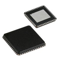
CYRF69103-40LFXC Cypress Semiconductor Corp, CYRF69103-40LFXC Datasheet - Page 7

CYRF69103-40LFXC
Manufacturer Part Number
CYRF69103-40LFXC
Description
IC PROC 8K FLASH 40VQFN
Manufacturer
Cypress Semiconductor Corp
Series
CYRFr
Datasheet
1.CYRF69103-40LFXC.pdf
(68 pages)
Specifications of CYRF69103-40LFXC
Package / Case
40-VQFN Exposed Pad, 40-HVQFN, 40-SQFN, 40-DHVQFN
Frequency
2.4GHz
Data Rate - Maximum
1Mbps
Modulation Or Protocol
ISM
Applications
General Purpose
Power - Output
6dBm
Sensitivity
-87dBm
Voltage - Supply
1.8 V ~ 3.6 V
Current - Receiving
21.9mA
Current - Transmitting
39.9mA
Data Interface
PCB, Surface Mount
Memory Size
8kB Flash, 256B SRAM
Antenna Connector
PCB, Surface Mount
Operating Temperature
0°C ~ 70°C
Processor Series
CYRF691x
Core
M8C
Data Bus Width
8 bit
Data Ram Size
256 B
Interface Type
SPI
Maximum Clock Frequency
2 MHz
Number Of Programmable I/os
15
Number Of Timers
4
Operating Supply Voltage
2.5 V, 3.3 V
Maximum Operating Temperature
+ 70 C
Mounting Style
SMD/SMT
Minimum Operating Temperature
0 C
Program Memory Type
Flash
Program Memory Size
8 KB
Operating Temperature (min)
0C
Operating Temperature (max)
70C
Operating Temperature Classification
Commercial
Operating Supply Voltage (min)
1.8V
Operating Supply Voltage (typ)
2.5/3.3V
Operating Supply Voltage (max)
3.6V
Height
1 mm
Length
5.9 mm
Supply Voltage (max)
3.6 V
Supply Voltage (min)
1.8 V
Width
5.9 mm
Lead Free Status / RoHS Status
Lead free / RoHS Compliant
For Use With
770-1001 - ISP 4PORT CYPRESS ENCORE II MCU
Lead Free Status / Rohs Status
Lead free / RoHS Compliant
Other names
428-1933
Available stocks
Company
Part Number
Manufacturer
Quantity
Price
Part Number:
CYRF69103-40LFXC
Manufacturer:
CYCRESS
Quantity:
20 000
Table 7-1. Pin Definitions (continued)
8. Functional Block Overview
All the blocks that make up the PRoC LP are presented in this
section.
8.1 2.4 GHz Radio
The radio transceiver is a dual conversion low IF architecture
optimized for power and range/robustness. The radio employs
channel matched filters to achieve high performance in the
presence of interference. An integrated Power Amplifier (PA)
provides up to +4 dBm transmit power, with an output power
control range of 34 dB in seven steps. The supply current of the
device is reduced as the RF output power is reduced.
Table 8-1. Internal PA Output Power Step Table
8.2 Frequency Synthesizer
Before transmission or reception may commence, it is necessary
for the frequency synthesizer to settle. The settling time varies
depending on channel; 25 fast channels are provided with a
maximum settling time of 100 μs.
The “fast channels” (<100 μs settling time) are every 3
frequency, starting at 2400 MHz up to and including 2472 MHz
(that is, 0,3,6,9…….69 and 72).
Document #: 001-07611 Rev *F
Pin
31
32
33
34
35
36
37
38
39
40
41
42
PA Setting
7
6
5
4
3
2
1
0
Corner Tabs
PACTL
V
Name
E-pad
V
V
P1.6
RST
P1.7
P0.7
DD1.8
L/D
V
REG
bat0
IO
Typical Output Power (dBm)
Control for external PA or Radio GPIO
GPIO
1.8V to 3.6V to main power supply rail for Radio I/O
Radio Reset. Connected to pin 40 with 0.47 μF. Must have a RST=HIGH event the very first time
power is applied to the radio otherwise the state of the radio control registers is unknown
GPIO
Regulated logic bypass. Connected to 0.47 μF to GND
Inductor/Diode connection for Boost. When Internal PMU is not being used connect L/D to GND.
GPIO
Connected to1.8V to 3.6V main power supply, through 0.047 μF bypass C
Boost regulator output voltage feedback
Must be connected to ground
Do Not connect corner tabs
–10
–15
–20
–25
–30
+4
–5
0
rd
8.3 Baseband and Framer
The baseband and framer blocks provide the DSSS encoding
and decoding, SOP generation and reception and CRC16
generation and checking, and EOP detection and length field.
8.3.1 Data Transmission Modes and Data Rates
The SoC supports four different data transmission modes:
■
■
■
■
Both 64-chip and 32-chip DATA_CODE_ADR codes are
supported. The four data transmission modes apply to the data
after the SOP. In particular the length, data, and CRC16 are all
sent in the same mode. In general, lower data rates reduces
packet error rate in any given environment.
The CYRF69103 IC supports the following data rates:
■
■
■
■
■
■
Lower data rates typically provide longer range and/or a more
robust link.
In GFSK mode, data is transmitted at 1 Mbps, without any
DSSS.
In 8DR mode, 8 bits are encoded in each DATA_CODE_ADR
derived code symbol transmitted.
In DDR mode, 2 bits are encoded in each DATA_CODE_ADR
derived code symbol transmitted (as in the CYWUSB6934 DDR
mode).
In SDR mode, 1 bit is encoded in each DATA_CODE_ADR
derived code symbol transmitted (as in the CYWUSB6934
standard modes).
1000 kbps (GFSK)
250 kbps (32-chip 8DR)
125 kbps (64-chip 8DR)
62.5 kbps (32-chip DDR)
31.25 kbps (64-chip DDR)
15.625 kbps (64-chip SDR)
Description
CYRF69103
Page 7 of 68
[+] Feedback


