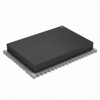
ATZB-900-B0 Atmel, ATZB-900-B0 Datasheet - Page 14

ATZB-900-B0
Manufacturer Part Number
ATZB-900-B0
Description
KIT MOD 802.15.4/ZIGB 900MHZ RF
Manufacturer
Atmel
Datasheet
1.ATZB-900-B0R.pdf
(20 pages)
Specifications of ATZB-900-B0
Frequency
779MHz ~ 787MHz, 868MHz ~ 868.6MHz, 902MHz ~ 928MHz
Data Rate - Maximum
250kbps
Modulation Or Protocol
802.15.4 Zigbee
Applications
Home/Building Automation, Industrial Control and Monitoring
Power - Output
11dBm
Sensitivity
-110dBm
Voltage - Supply
1.8 V ~ 3.6 V
Current - Receiving
15mA
Current - Transmitting
20mA
Data Interface
PCB, Surface Mount
Memory Size
128kBytes Flash, 8kBytes RAM, 4kBytes EEPROM
Antenna Connector
PCB, Surface Mount
Operating Temperature
-40°C ~ 85°C
Package / Case
Module
Lead Free Status / RoHS Status
Lead free / RoHS Compliant
Available stocks
Company
Part Number
Manufacturer
Quantity
Price
Company:
Part Number:
ATZB-900-B0R
Manufacturer:
SANREX
Quantity:
82
Part Number:
ATZB-900-B0R
Manufacturer:
ATMEL/爱特梅尔
Quantity:
20 000
ZigBit™ 700/800/900 MHz Wireless Modules
Table 3-6. Pin descriptions (Continued)
Notes:
Connector
44,46,48
24,25
Pin
16
17
18
19
20
21
26
27
28
29
30
31
32
33
34
35
36
37
38
39
40
41
42
43
45
47
1. The UART_TXD pin is intended for input (i.e. its designation as "TXD" implies some complex system
2. Most of pins can be configured for general purpose I/O or for some alternate functions as described in
3. GPIO pins can be programmed either for output, or for input with/without pull-up resistors. Output pin
4. All digital pins are provided with protection diodes to D_VCC and DGND
containing ZigBit 900 as its RF terminal unit), while UART_RXD pin, vice versa, is for output.
details in the ATmega1281V Datasheet [1].
drivers are strong enough to drive LED displays directly (refer to figures on pages 387-388, [1]).
USART0_EXTCLK
ADC_INPUT_3
ADC_INPUT_2
ADC_INPUT_1
USART0_RXD
USART0_TXD
UART_CTS
GPIO_1WR
UART_DTR
JTAG_TMS
JTAG_TDO
JTAG_TCK
Pin Name
JTAG_TDI
A_VREF
RF GND
RFP_IO
RFN_IO
D_VCC
GPIO6
GPIO7
GPIO3
GPIO4
GPIO5
GPIO8
AGND
IRQ_7
IRQ_6
BAT
General Purpose Digital Input/Output 8
CTS output (Clear To send) for UART hardware
General Purpose digital Input/Output 6
General Purpose digital Input/Output 7
General Purpose digital Input/Output 3
General Purpose digital Input/Output 4
General Purpose digital Input/Output 5
measurement. This pin equals V
DTR input (Data Terminal Ready) for UART.
ADC Input Channel 0, used for battery level
Digital Input Interrupt request 7
Digital Input Interrupt request 6
Input/Output reference voltage for ADC
USART/SPI External Clock
USART /SPI Transmit pin
USART/SPI Receive pin
JTAG Test Mode Select
JTAG Test Data Output
flow control. Active low
Digital Supply Voltage (V
JTAG Test Data Input
ADC Input Channel 3
ADC Input Channel 2
ADC Input Channel 1
Differential RF Input/Output
Differential RF Input/Output
JTAG Test Clock
1-wire interface
Active low
RF Analog Ground
Analog ground
Description
(2)(3)(4)(7)
(2)(3)(4)(7)
(2)(3)(4)(6)
(2)(3)(4)(6)
(2)(3)(4)(7)
(2)(3)(4)(6)
(2)(3)(4)(6)
(2)(3)(7)
(2)(3)(7)
(2)(3)(7)
(2)(3)(4)(7)
(2)(3)(4)(7)
(2)(3)(4)(7)
CC
CC
(2)(3)(4)(7)
(2)(3)(4)(7)
)
(9)
/3.
(2)(3)(4)(7)
(2)(3)(4)(7)
(2)(3)(4)(7)
(2)(3)(4)(7)
(2)(3)(4)(7)
(2)(3)(4)(7)
(2)(3)(7)
8227C–MCU Wireless–06/09
I/O
I/O
I/O
I/O
I/O
I/O
I/O
I/O
I/O
I/O
I/O
I/O
O
O
O
I
I
I
I
I
I
I
I
I
I
I
Specifications
State after
Power on
Default
tri-state
tri-state
tri-state
tri-state
tri-state
tri-state
tri-state
tri-state
tri-state
tri-state
tri-state
tri-state
tri-state
tri-state
tri-state
tri-state
tri-state
tri-state
3-7


