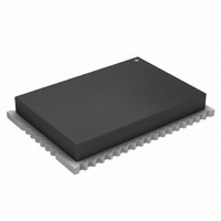
ATZB-900-B0 Atmel, ATZB-900-B0 Datasheet - Page 15

ATZB-900-B0
Manufacturer Part Number
ATZB-900-B0
Description
KIT MOD 802.15.4/ZIGB 900MHZ RF
Manufacturer
Atmel
Datasheet
1.ATZB-900-B0R.pdf
(20 pages)
Specifications of ATZB-900-B0
Frequency
779MHz ~ 787MHz, 868MHz ~ 868.6MHz, 902MHz ~ 928MHz
Data Rate - Maximum
250kbps
Modulation Or Protocol
802.15.4 Zigbee
Applications
Home/Building Automation, Industrial Control and Monitoring
Power - Output
11dBm
Sensitivity
-110dBm
Voltage - Supply
1.8 V ~ 3.6 V
Current - Receiving
15mA
Current - Transmitting
20mA
Data Interface
PCB, Surface Mount
Memory Size
128kBytes Flash, 8kBytes RAM, 4kBytes EEPROM
Antenna Connector
PCB, Surface Mount
Operating Temperature
-40°C ~ 85°C
Package / Case
Module
Lead Free Status / RoHS Status
Lead free / RoHS Compliant
Available stocks
Company
Part Number
Manufacturer
Quantity
Price
Company:
Part Number:
ATZB-900-B0R
Manufacturer:
SANREX
Quantity:
82
Part Number:
ATZB-900-B0R
Manufacturer:
ATMEL/爱特梅尔
Quantity:
20 000
ZigBit™ 700/800/900 MHz Wireless Modules
5. It is strongly recommended to avoid assigning an alternate function for OSC32K_OUT pin because it is
6. Normally, JTAG_TMS, JTAG_TDI, JTAG_TDO, JTAG_TCK pins are used for on-chip debugging and
7. The following pins can be configured with the BitCloud software to be general-purpose I/O lines:
8. With BitCloud, CTS pin can be configured to indicate sleep/active condition of the module thus provid-
9. Using ferrite bead and 1 µF capacitor located closely to the power supply pin is recommended, as
10. In SPI mode, USART0_EXTCLK is output. In USART mode, this pin can be configured as either input or
used by BitCloud. However, this signal can be used if another peripheral or host processor requires
32.768 kHz clock, otherwise this pin can be disconnected.
flash burning. They can be used for A/D conversion if JTAGEN fuse is disabled.
GPIO0, GPIO1, GPIO2, GPIO3, GPIO4, GPIO5, GPIO6, GPIO7, GPIO8, GPIO_1WR, I2C_CLK,
I2C_DATA, UART_TXD, UART_RXD, UART_RTS, UART_CTS, ADC_INPUT_3, ADC_INPUT_2,
ADC_INPUT_1, BAT, UART_DTR, USART0_RXD, USART0_TXD, USART0_EXTCLK, IRQ_7, IRQ_6.
Additionally, four JTAG lines can be programmed with software as GPIO as well, but this requires
changing the fuse bits and will disable JTAG debugging.
ing mechanism for power management of host processor. If this function is necessary, connection of
this pin to external pull-down resistor is recommended to prevent the undesirable transients during
module reset process.
shown below.
output pin.
8227C–MCU Wireless–06/09
Specifications
3-8


