XBP24-ASI-001 Digi International, XBP24-ASI-001 Datasheet - Page 8
XBP24-ASI-001
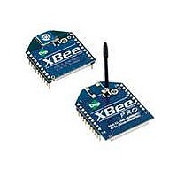
Manufacturer Part Number
XBP24-ASI-001
Description
MODULE XBEE 1MW W/RPSMA
Manufacturer
Digi International
Series
XBEE-PRO™r
Specifications of XBP24-ASI-001
Frequency
2.4GHz
Data Rate - Maximum
250kbps
Modulation Or Protocol
802.15.4
Applications
Home/Building Automation, Industrial Control, ZigBee™
Power - Output
18dBm
Sensitivity
-100dBm
Voltage - Supply
2.8 V ~ 3.4 V
Current - Receiving
55mA
Current - Transmitting
215mA @ 3.3V
Data Interface
PCB, Through Hole
Antenna Connector
RP-SMA
Operating Temperature
-40°C ~ 85°C
Package / Case
Module
Lead Free Status / RoHS Status
Lead free / RoHS Compliant
Memory Size
-
Lead Free Status / Rohs Status
Lead free / RoHS Compliant
Available stocks
Company
Part Number
Manufacturer
Quantity
Price

Part Number:
XBP24-ASI-001J
Manufacturer:
XBEE
Quantity:
20 000


XBee®/XBee‐PRO® RF Modules ‐ 802.15.4 ‐ v1.xEx [2009.09.23]
Table 1‐03. DC Characteristics (VCC = 2.8 ‐ 3.4 VDC)
Table 1‐04. ADC Characteristics (Operating)
Table 1‐05. ADC Timing/Performance Characteristics
PWR-DWN
Electrical Characteristics
Symbol
Symbol
Symbol
1. Maximum electrical operating range, not valid conversion range.
* V
1. All ACCURACY numbers are based on processor and system being in WAIT state (very little activity and no IO switching)
and that adequate low‐pass filtering is present on analog input pins (filter with 0.01 μF to 0.1 μF capacitor between analog
input and VREFL). Failure to observe these guidelines may result in system or microcontroller noise causing accuracy errors
which will vary based on board layout and the type and magnitude of the activity.
Data transmission and reception during data conversion may cause some degradation of these specifications, depending on
the number and timing of packets. It is advisable to test the ADCs in your installation if best accuracy is required.
2. R
not fully charge the input circuitry of the ATD resulting in accuracy error.
3. Analog input must be between V
4. The resolution is the ideal step size or 1LSB = (V
5. Differential non‐linearity is the difference between the current code width and the ideal code width (1LSB). The current
code width is the difference in the transition voltages to and from the current code.
6. Integral non‐linearity is the difference between the transition voltage to the current code and the adjusted ideal transition
voltage for the current code. The adjusted ideal transition voltage is (Current Code–1/2)*(1/((V
7. Zero‐scale error is the difference between the transition to the first valid code and the ideal transition to that code. The
Ideal transition voltage to a given code is (Code–1/2)*(1/(V
8. Full‐scale error is the difference between the transition to the last valid code and the ideal transition to that code. The ideal
transition voltage to a given code is (Code–1/2)*(1/(V
9. Input leakage error is error due to input leakage across the real portion of the impedance of the network driving the analog
pin. Reducing the impedance of the network reduces this error.
V
V
V
RES
DNL
V
V
I
R
E
II
INL
E
F
V
V
II
RX
REFH
E
TX
REF
INDC
AIN
OH
OZ
OL
IN
AS
ZS
FS
TU
IH
DDAD
IL
IL
AS
is the real portion of the impedance of the network driving the analog input pin. Values greater than this amount may
is connected to VCC.
VREF - Analog-to-Digital converter
High Impedance Leakage Current
VREF - Reference Supply Current
Source Impedance at Input
Ideal Resolution (1 LSB)
Differential Non-linearity
Total Unadjusted Error
Input Leakage Current
Analog Input Voltage
Analog Input Voltage
Integral Non-linearity
Input Leakage Error
Power-down Current
Output High Voltage
Output Low Voltage
Input High Voltage
Input Low Voltage
Characteristic
Characteristic
Characteristic
Zero-scale Error
Transmit Current
Receive Current
Full-scale Error
reference range
© 2009 Digi Internatonal, Inc.
8
7
9
1
3
6
10
5
4
2
REFL
and V
V
IN
V
IN
= VCC or GND, all I/O High-Z, per pin
Disabled or Sleep Mode
2.08V < V
= VCC or GND, all inputs, per pin
I
REFH
OH
I
OL
Condition
Condition
= 2 mA, VCC >= 2.7 V
= -2 mA, VCC >= 2.7 V
SM parameter = 1
for valid conversion. Values greater than V
REFH
All Digital Inputs
All Digital Inputs
Enabled
VCC = 3.3 V
VCC = 3.3 V
REFH
Condition
1
DDAD
–V
–V
REFL
REFH
< 3.6V
REFL
)/1024
–V
)).
REFL
)).
V
SSAD
V
2.031
2.08
Min
Min
REFL
0.7 * VCC
VCC - 0.5
-
-
-
-
-
-
-
-
-
- 0.3
Min
-
-
-
-
-
-
-
(XBee)
(XBee)
45
50
Typical
Typical
< 0.01
±0.05
±0.5
±0.5
±0.4
±0.4
±1.1
200
Typical
REFH
REFH
-
-
-
-
0.025
0.025
< 10
-
-
-
-
will convert to $3FF.
+E
215, 140
(PRO)
(PRO,
FS
Int)
55
)–(V
V
REFL
DDAD
V
0.35 * VCC
V
3.516
Max
Max
±1.0
±1.0
±1.0
±1.0
±5.0
±2.5
DDAD*
0.02
REFH
+E
10
-
Max
0.5
+ 0.3
1
1
ZS
-
-
-
-
-
))).
Unit
Unit
Unit
LSB
LSB
LSB
LSB
LSB
LSB
mA
mA
8
µA
µA
µA
mV
µA
µA
k
V
V
V
V
V
V
V
Related parts for XBP24-ASI-001
Image
Part Number
Description
Manufacturer
Datasheet
Request
R

Part Number:
Description:
MODULE 802.15.4 100MW CHIP ANT
Manufacturer:
Digi International/Maxstream
Datasheet:
Part Number:
Description:
MODULE 802.15.4 RS-232 ANT
Manufacturer:
Digi International/Maxstream
Datasheet:
Part Number:
Description:
MODULE XBEE PRO ZNET 2.5 W/RPSMA
Manufacturer:
Digi International/Maxstream
Datasheet:
Part Number:
Description:
KIT STARTER XBEE PRO
Manufacturer:
Digi International/Maxstream
Datasheet:
Part Number:
Description:
MODULE 802.15.4 100MW WIRE ANT
Manufacturer:
Digi International/Maxstream
Datasheet:
Part Number:
Description:
MODULE 802.15.4 100MW U.FL CON
Manufacturer:
Digi International/Maxstream
Datasheet:
Part Number:
Description:
MODULE XBEE PRO ZNET 2.5 W/CHIP
Manufacturer:
Digi International/Maxstream
Datasheet:
Part Number:
Description:
MODULE XBEE PRO ZNET 2.5 W/WHIP
Manufacturer:
Digi International/Maxstream
Datasheet:

Part Number:
Description:
MODULE ZIGBEE-PRO W/WIRED ANT
Manufacturer:
Digi International
Datasheet:
Part Number:
Description:
MODULE ZIGBEE-PRO W/RPSMA ANT
Manufacturer:
Digi International
Datasheet:
Part Number:
Description:
IC ARM MICROPROCESSOR 177BGA
Manufacturer:
Digi International
Datasheet:
Part Number:
Description:
DIGI CONNECT 4MB FLASH 8MB RAM
Manufacturer:
Digi International
Datasheet:

Part Number:
Description:
ME 8MB SDRAM 2MB FLASH SINGLE
Manufacturer:
Digi International
Datasheet:
Part Number:
Description:
ME 8MB SDRAM 2MB FLASH SINGLE
Manufacturer:
Digi International
Datasheet:

Part Number:
Description:
MODULE 9P 8MB SDRAM 4MB FLASH
Manufacturer:
Digi International/Maxstream
Datasheet: