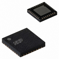
PN5120A0HN1/C1,151 NXP Semiconductors, PN5120A0HN1/C1,151 Datasheet - Page 8

PN5120A0HN1/C1,151
Manufacturer Part Number
PN5120A0HN1/C1,151
Description
IC TRANSMISSION MOD 32-HVQFN
Manufacturer
NXP Semiconductors
Datasheet
1.PN5120A0HN1C1118.pdf
(23 pages)
Specifications of PN5120A0HN1/C1,151
Package / Case
32-VQFN Exposed Pad, 32-HVQFN, 32-SQFN, 32-DHVQFN
Rf Type
Read / Write
Frequency
13.56MHz
Features
ISO14443A, ISO1443B
Operating Frequency
13.56 MHz
Supply Voltage (max)
3.6 V
Supply Voltage (min)
2.5 V
Supply Current
7 mA
Maximum Power Dissipation
200 mW
Operating Temperature Range
- 30 C to + 85 C
Maximum Operating Temperature
+ 85 C
Minimum Operating Temperature
- 30 C
Mounting Style
SMD/SMT
Lead Free Status / RoHS Status
Lead free / RoHS Compliant
Lead Free Status / RoHS Status
Lead free / RoHS Compliant, Lead free / RoHS Compliant
Other names
935280537151
PN5120A0HN1/C1-S
PN5120A0HN1/C1-S
PN5120A0HN1/C1-S
PN5120A0HN1/C1-S
NXP Semiconductors
Table 3.
124533
Product short data sheet
Symbol
A1
PVDD
DVDD
DVSS
PVSS
NRSTPD
SIGIN
SIGOUT
SVDD
TVSS
TX1
TVDD
TX2
TVSS
AVDD
VMID
RX
AVSS
AUX1
AUX2
OSCIN
OSCOUT
IRQ
ALE
D1 to D7
A0
Pin description HVQFN32
Pin
1
2
3
4
5
6
7
8
9
10
11
12
13
14
15
16
17
18
19
20
21
22
23
24
25 to 31
32
7.2 Pin description
Type
I
PWR
PWR
PWR
PWR
I
I
O
PWR
PWR
O
PWR
O
PWR
PWR
PWR
I
PWR
O
O
I
O
O
I
I/O
I
Description
Address Line
Pad power supply
Digital Power Supply
Digital Ground
Pad power supply ground
Not Reset and Power Down: When LOW, internal current sinks are switched off, the
oscillator is inhibited, and the input pads are disconnected from the outside world. With
a positive edge on this pin the internal reset phase starts.
Communication Interface Input: accepts a digital, serial data stream
Communication Interface Output: delivers a serial data stream
S
Transmitter Ground: supplies the output stage of TX1 and TX2
Transmitter 1: delivers the modulated 13.56 MHz energy carrier
Transmitter Power Supply: supplies the output stage of TX1 and TX2
Transmitter 2: delivers the modulated 13.56 MHz energy carrier
Transmitter Ground: supplies the output stage of TX1 and TX2
Analog Power Supply
Internal Reference Voltage: This pin delivers the internal reference voltage.
Receiver Input
Analog Ground
Auxiliary Outputs: These pins are used for testing.
Crystal Oscillator Input: input to the inverting amplifier of the oscillator. This pin is
also the input for an externally generated clock (f
Crystal Oscillator Output: Output of the inverting amplifier of the oscillator.
Interrupt Request: output to signal an interrupt event
Address Latch Enable: signal to latch AD0 to AD5 into the internal address latch
when HIGH.
8-bit Bi-directional Data Bus.
Remark: An 8-bit parallel interface is not available.
Remark: If the host controller selects I
can be used to define the I
Remark: For serial interfaces this pins can be used for test signals or I/Os.
Address Line
2
C Pad Power Supply: provides power to the S
Rev. 3.3 — 13 June 2007
2
C address.
2
C as digital host controller interface, these pins
osc
2
C pads
= 27.12 MHz).
Transmission Module
© NXP B.V. 2007. All rights reserved.
PN512
8 of 23


