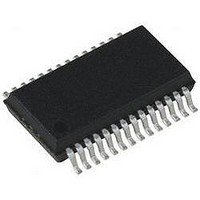
PIC18LF24K22-I/SS Microchip Technology, PIC18LF24K22-I/SS Datasheet - Page 139

PIC18LF24K22-I/SS
Manufacturer Part Number
PIC18LF24K22-I/SS
Description
IC PIC MCU 16KB FLASH 28SSOP
Manufacturer
Microchip Technology
Series
PIC® XLP™ 18Fr
Specifications of PIC18LF24K22-I/SS
Core Size
8-Bit
Program Memory Size
16KB (8K x 16)
Core Processor
PIC
Speed
64MHz
Connectivity
I²C, SPI, UART/USART
Peripherals
Brown-out Detect/Reset, HLVD, POR, PWM, WDT
Number Of I /o
24
Program Memory Type
FLASH
Eeprom Size
256 x 8
Ram Size
768 x 8
Voltage - Supply (vcc/vdd)
1.8 V ~ 3.6 V
Data Converters
A/D 19x10b
Oscillator Type
Internal
Operating Temperature
-40°C ~ 85°C
Package / Case
28-SSOP (0.200", 5.30mm Width)
Controller Family/series
PIC18
No. Of I/o's
25
Eeprom Memory Size
256Byte
Ram Memory Size
768Byte
Cpu Speed
64MHz
No. Of Timers
7
Lead Free Status / RoHS Status
Lead free / RoHS Compliant
- Current page: 139 of 496
- Download datasheet (5Mb)
A mismatch condition will continue to set the RBIF flag bit.
Reading or writing PORTB will end the mismatch
condition and allow the RBIF bit to be cleared. The latch
holding the last read value is not affected by a MCLR nor
Brown-out Reset. After either one of these Resets, the
RBIF flag will continue to be set if a mismatch is present.
The interrupt-on-change feature is recommended for
wake-up on key depression operation and operations
where PORTB is only used for the interrupt-on-change
feature. Polling of PORTB is not recommended while
using the interrupt-on-change feature.
TABLE 10-5:
2010 Microchip Technology Inc.
RB0/INT0/CCP4/
FLT0/SRI/SS2/
AN12
RB1/INT1/P1C/
SCK2/SCL2/
C12IN3-/AN10
Legend:
Note 1:
Note:
2:
3:
Pin
AN = Analog input or output; TTL = TTL compatible input; HV = High Voltage; OD = Open Drain; XTAL = Crystal; CMOS =
CMOS compatible input or output; ST = Schmitt Trigger input with CMOS levels; I
Default pin assignment for P2B, T3CKI, CCP3 and CCP2 when Configuration bits PB2MX, T3CMX, CCP3MX and
CCP2MX are set.
Alternate pin assignment for P2B, T3CKI, CCP3 and CCP2 when Configuration bits PB2MX, T3CMX, CCP3MX and
CCP2MX are clear.
Function on PORTD and PORTE for PIC18(L)F4XK22 devices.
If a change on the I/O pin should occur
when the read operation is being executed
(start of the Q2 cycle), then the RBIF
interrupt flag may not get set. Furthermore,
since a read or write on a port affects all
bits of that port, care must be taken when
using multiple pins in Interrupt-on-change
mode. Changes on one pin may not be
seen while servicing changes on another
pin.
PORTB I/O SUMMARY
Function
C12IN3-
CCP4
SCK2
SCL2
SS2
P1C
AN12
AN10
FLT0
INT0
INT1
RB0
RB1
SRI
(3)
(3)
(3)
(3)
(3)
Setting
TRIS
0
1
1
0
1
1
1
1
1
0
1
1
0
0
1
0
1
1
1
ANSEL
Setting
0
0
0
0
0
0
0
0
1
0
0
0
0
0
0
0
0
1
1
Type
Pin
Preliminary
O
O
O
O
O
O
I
I
I
I
I
I
I
I
I
I
I
I
I
Buffer
Type
DIG
TTL
DIG
TTL
DIG
DIG
DIG
DIG
AN
I
AN
AN
ST
ST
ST
ST
ST
ST
ST
2
C
10.3.3
PORTB is multiplexed with several peripheral functions
(Table
these pin functions can be relocated to alternate pins
using the Control fuse bits in CONFIG3H. RB5 is the
default pin for P2B (28-pin devices). Clearing the
P2BMX bit moves the pin function to RC0. RB5 is also
the default pin for the CCP3/P3A peripheral pin. Clear-
ing the CCP3MX bit moves the pin function to the RC6
pin (28-pin devices) or RE0 (40/44-pin devices).
Two other pin functions, T3CKI and CCP2/P2A, can be
relocated from their default pins to PORTB pins by
clearing the control fuses in CONFIG3H. Clearing
T3CMX and CCP2MX moves the pin functions to RB5
and RB3, respectively.
LATB<0> data output; not affected by analog input.
PORTB<0> data input; disabled when analog input
enabled.
External interrupt 0.
Compare 4 output/PWM 4 output.
Capture 4 input.
PWM Fault input for ECCP auto-shutdown.
SR Latch input.
SPI slave select input (MSSP2).
Analog input 12.
LATB<1> data output; not affected by analog input.
PORTB<1> data input; disabled when analog input
enabled.
External Interrupt 1.
Enhanced CCP1 PWM output 3.
MSSP2 SPI Clock output.
MSSP2 SPI Clock input.
MSSP2 I
MSSP2 I
Comparators C1 and C2 inverting input.
Analog input 10.
PIC18(L)F2X/4XK22
10-5). The pins have TTL input buffers. Some of
2
2
C
C
TM
TM
ALTERNATE FUNCTIONS
Clock output.
Clock input.
2
C
TM
Description
=
Schmitt Trigger input with I
DS41412D-page 139
2
C.
Related parts for PIC18LF24K22-I/SS
Image
Part Number
Description
Manufacturer
Datasheet
Request
R

Part Number:
Description:
Manufacturer:
Microchip Technology Inc.
Datasheet:

Part Number:
Description:
Manufacturer:
Microchip Technology Inc.
Datasheet:

Part Number:
Description:
Manufacturer:
Microchip Technology Inc.
Datasheet:

Part Number:
Description:
Manufacturer:
Microchip Technology Inc.
Datasheet:

Part Number:
Description:
Manufacturer:
Microchip Technology Inc.
Datasheet:

Part Number:
Description:
Manufacturer:
Microchip Technology Inc.
Datasheet:

Part Number:
Description:
Manufacturer:
Microchip Technology Inc.
Datasheet:

Part Number:
Description:
Manufacturer:
Microchip Technology Inc.
Datasheet:


