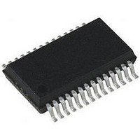
PIC18LF24K22-I/SS Microchip Technology, PIC18LF24K22-I/SS Datasheet - Page 339

PIC18LF24K22-I/SS
Manufacturer Part Number
PIC18LF24K22-I/SS
Description
IC PIC MCU 16KB FLASH 28SSOP
Manufacturer
Microchip Technology
Series
PIC® XLP™ 18Fr
Specifications of PIC18LF24K22-I/SS
Core Size
8-Bit
Program Memory Size
16KB (8K x 16)
Core Processor
PIC
Speed
64MHz
Connectivity
I²C, SPI, UART/USART
Peripherals
Brown-out Detect/Reset, HLVD, POR, PWM, WDT
Number Of I /o
24
Program Memory Type
FLASH
Eeprom Size
256 x 8
Ram Size
768 x 8
Voltage - Supply (vcc/vdd)
1.8 V ~ 3.6 V
Data Converters
A/D 19x10b
Oscillator Type
Internal
Operating Temperature
-40°C ~ 85°C
Package / Case
28-SSOP (0.200", 5.30mm Width)
Controller Family/series
PIC18
No. Of I/o's
25
Eeprom Memory Size
256Byte
Ram Memory Size
768Byte
Cpu Speed
64MHz
No. Of Timers
7
Lead Free Status / RoHS Status
Lead free / RoHS Compliant
- Current page: 339 of 496
- Download datasheet (5Mb)
22.0
The Digital-to-Analog Converter supplies a variable
voltage reference, ratiometric with the input source,
with 32 selectable output levels.
The input of the DAC can be connected to:
• External V
• V
• FVR (Fixed Voltage Reference)
The output of the DAC can be configured to supply a
reference voltage to the following:
• Comparator positive input
• ADC input channel
• DACOUT pin
The Digital-to-Analog Converter (DAC) can be enabled
by setting the DACEN bit of the VREFCON1 register.
22.1
The DAC has 32 voltage level ranges. The 32 levels
are set with the DACR<4:0> bits of the VREFCON2
register.
The DAC output voltage is determined by the following
equations:
EQUATION 22-1:
22.2
The DAC output value is derived using a resistor ladder
with each end of the ladder tied to a positive and
negative voltage reference input source. If the voltage
of either input source fluctuates, a similar fluctuation will
result in the DAC output value.
The value of the individual resistors within the ladder
can
Characteristics”.
22.3
In order for the DAC module to consume the least
amount of power, one of the two voltage reference input
sources to the resistor ladder must be disconnected.
Either the positive voltage source, (V
negative voltage source, (V
2010 Microchip Technology Inc.
V
DD
V
V
SRC
SRC
OUT
supply voltage
be
+ = V
- = V
DIGITAL-TO-ANALOG
CONVERTER (DAC) MODULE
Output Voltage Selection
Ratiometric Output Level
Low-Power Voltage State
=
REF
found
V
DD
SS
SRC
or V
, V
pins
+ V
REF
REF
–
+ or FVR1
in
DAC OUTPUT VOLTAGE
-
SRC
-
Section 27.0
SRC
DACR<4:0>
------------------------------ -
-) can be disabled.
2 5
SRC
+ V
“Electrical
+), or the
SRC
-
Preliminary
The negative voltage source is disabled by setting the
DACLPS bit in the VREFCON1 register. Clearing the
DACLPS bit in the VREFCON1 register disables the
positive voltage source.
22.4
The DAC output voltage can be set to V
least amount of power consumption by performing the
following:
• Clearing the DACEN bit in the VREFCON1
• Setting the DACLPS bit in the VREFCON1
• Configuring the DACPSS bits to the proper
• Configuring the DACRx bits to ‘11111’ in the
This is also the method used to output the voltage level
from the FVR to an output pin. See
Voltage Reference Output”
22.5
The DAC output voltage can be set to V
least amount of power consumption by performing the
following:
• Clearing the DACEN bit in the VREFCON1
• Clearing the DACLPS bit in the VREFCON1
• Configuring the DACPSS bits to the proper
• Configuring the DACRx bits to ‘00000’ in the
This allows the comparator to detect a zero-crossing
while not consuming additional current through the DAC
module.
22.6
The DAC can be output to the DACOUT pin by setting
the DACOE bit of the VREFCON1 register to ‘1’.
Selecting the DAC reference voltage for output on the
DACOUT pin automatically overrides the digital output
buffer and digital input threshold detector functions of
that pin. Reading the DACOUT pin when it has been
configured for DAC reference voltage output will always
return a ‘0’.
Due to the limited current drive capability, a buffer must
be used on the DAC voltage reference output for
external connections to DACOUT.
an example buffering technique.
register.
register.
positive source.
VREFCON2 register.
register.
register.
negative source.
VREFCON2 register.
PIC18(L)F2X/4XK22
Output Clamped to Positive
Voltage Source
Output Clamped to Negative
Voltage Source
DAC Voltage Reference Output
for more information.
Section 22.6 “DAC
DS41412D-page 339
Figure 22-2
SRC
SRC
+ with the
- with the
shows
Related parts for PIC18LF24K22-I/SS
Image
Part Number
Description
Manufacturer
Datasheet
Request
R

Part Number:
Description:
Manufacturer:
Microchip Technology Inc.
Datasheet:

Part Number:
Description:
Manufacturer:
Microchip Technology Inc.
Datasheet:

Part Number:
Description:
Manufacturer:
Microchip Technology Inc.
Datasheet:

Part Number:
Description:
Manufacturer:
Microchip Technology Inc.
Datasheet:

Part Number:
Description:
Manufacturer:
Microchip Technology Inc.
Datasheet:

Part Number:
Description:
Manufacturer:
Microchip Technology Inc.
Datasheet:

Part Number:
Description:
Manufacturer:
Microchip Technology Inc.
Datasheet:

Part Number:
Description:
Manufacturer:
Microchip Technology Inc.
Datasheet:


